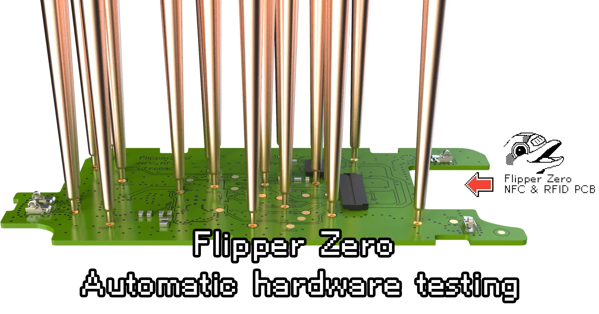
What testing electronics Flipper Zero looks like
Flipper Zero – a project of a pocket multitool for hackers in the Tamagotchi form factor, which we are developing. Previous Posts [1],[2],[3],[4],[5],[6],[7],[8],[9],[10],[11],[12],[13],[14],[15],[16]
The electronics and housings for the Flipper Zero are manufactured in different factories in China. Today we move to an electronics factory and see what automatic electronic testing of individual Flipper boards looks like.
There is always a defect in large volumes of electronics production. Some percentage of motherboards may not work stupidly, others may have a small, barely noticeable defect, such as impaired reception and transmission characteristics. It is important that defective Flippers do not leave for users. To do this, in production, all components undergo two stages of testing: electrical testing of each board separately and then testing the entire device as an assembly.
In this article, we will analyze the first stage – automatic electronic testing of individual Flipper Zero boards.
How Flipper Zero boards are made

Layout of PCBs inside Flipper Zero
Flipper consists of 4 boards
- NFC_RFID – this board contains 125 kHz RFID and 13.56 MHz NFC components
- Main PCB – the main board, which houses the STM32 microcontroller, display, Sub-1 GHz module and buttons
- iButton Infrared PCB – has pogo pins for iButton contacts, piezo speaker and IR receiver and transmitter module
- Antenna board – combined dual-band antenna for 125 kHz and 13.56 MHz, which is pressed against the NFC_RFID board
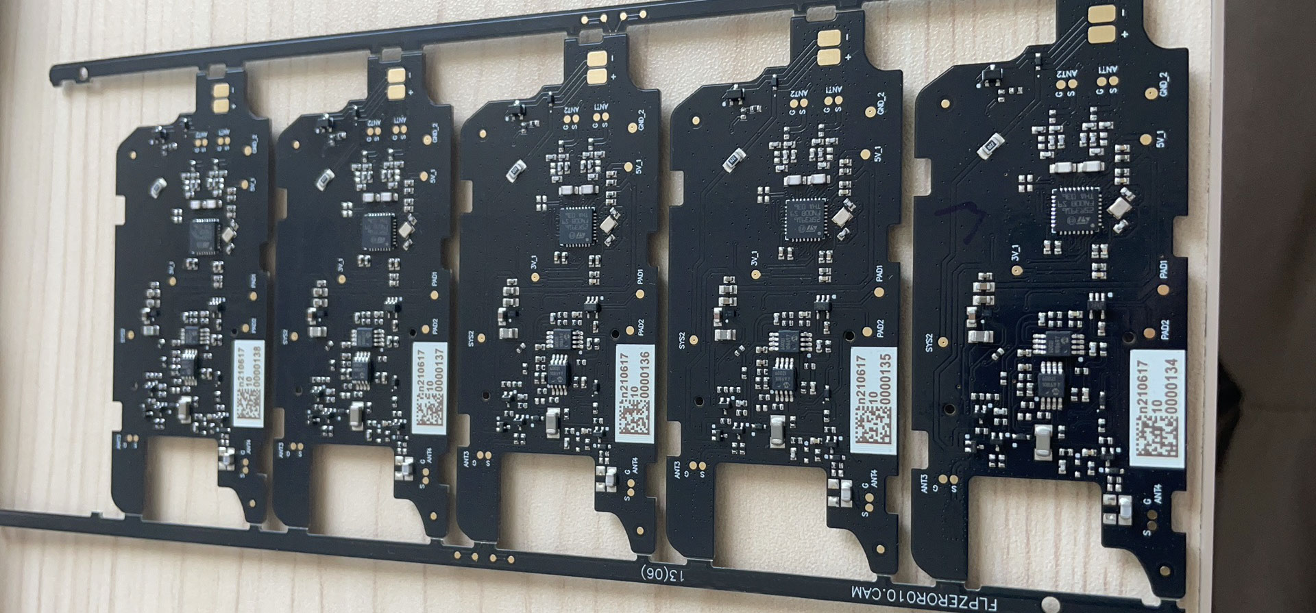
Each board is manufactured separately and tested separately. First, a bare PCB is produced. These are layers of textolite and copper foil, on which signal tracks and contact pads are etched. The PCB layers are glued together, and the contact tracks are connected between the layers using vias. The most complex flipper board is Main, it houses the STM32 microcontroller, display and buttons – it consists of 6 layers!
Bare Printed Circuit Boards Main PCB
Main PCB close-up
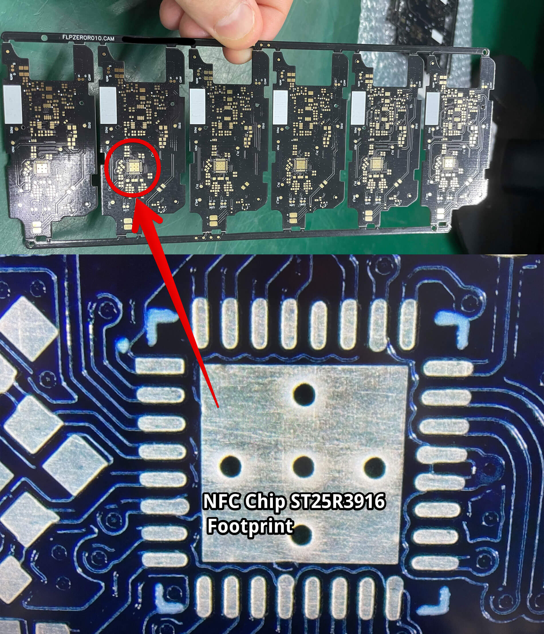
Bare NFC_RFID PCBs with no components mounted
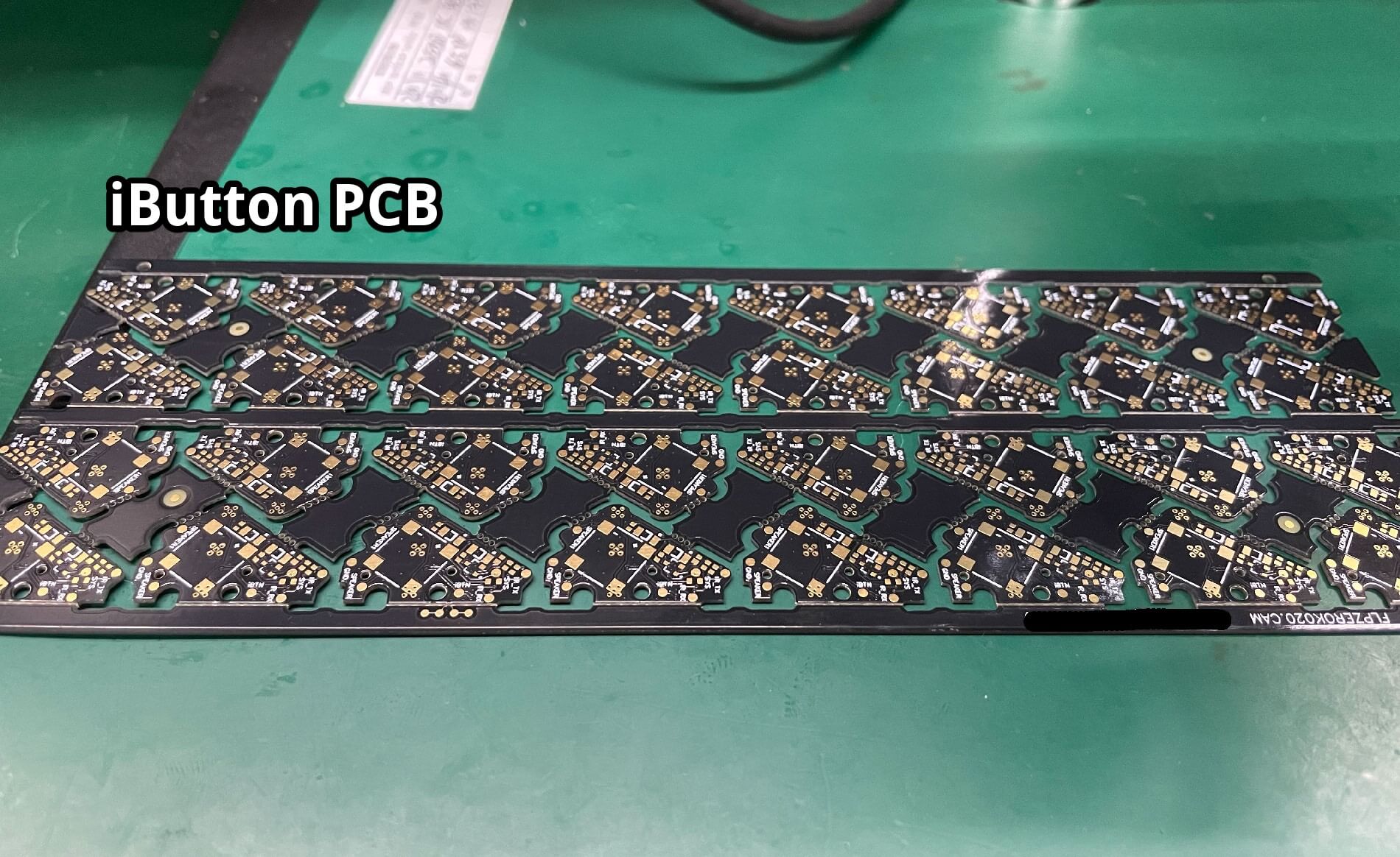
Bare PCB iButton
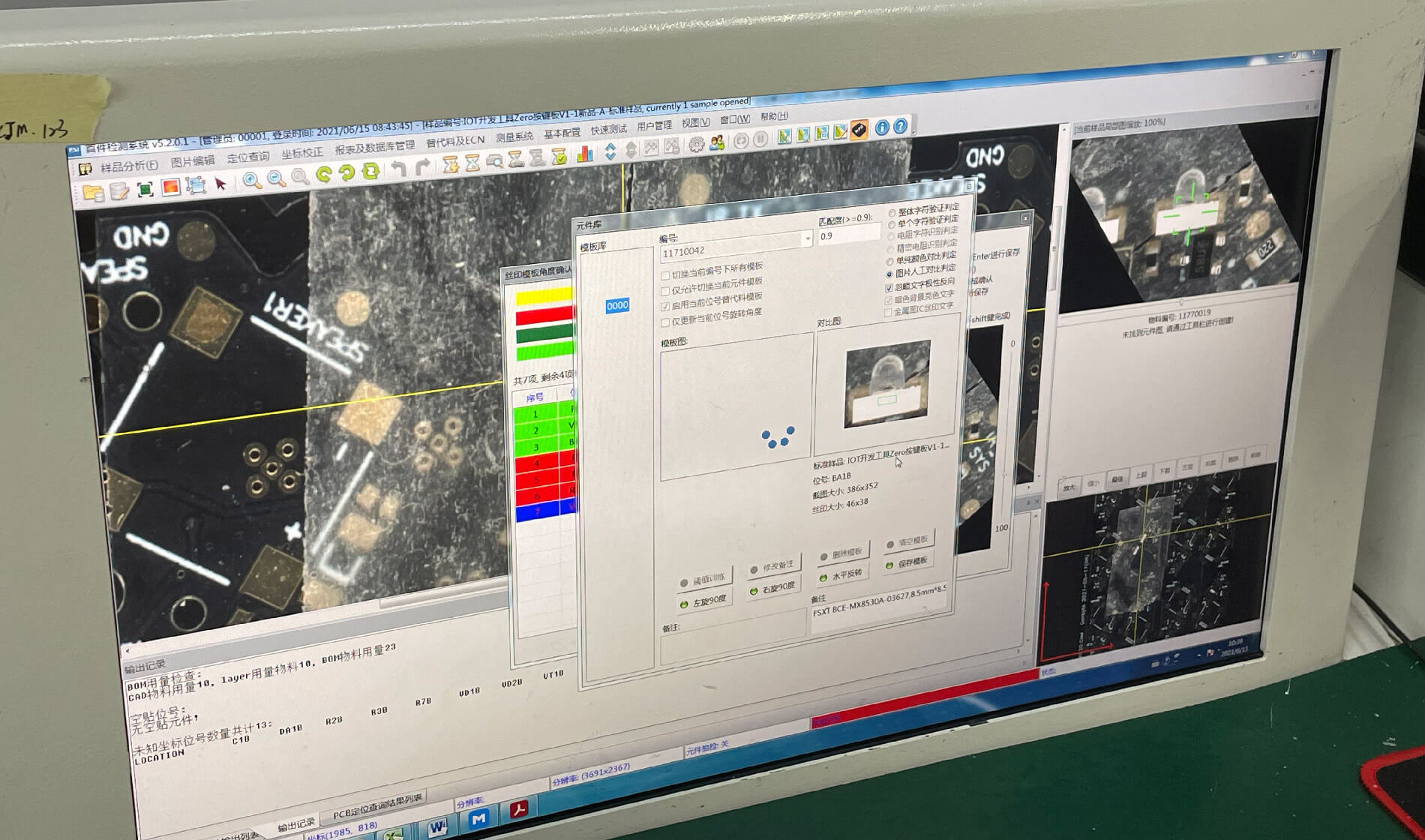
During the production of a printed circuit board, before assembling components, it undergoes visual analysis and electrical testing. Visual analysis takes place under a microscope, all contact pads are examined, a solder mask (paint that separates the soldering points from the rest of the board), silk screen printing, etc.
This step reveals manufacturing defects, for example, in our case, incorrect opening of the solder mask on the Main board. The place for the BGA component was completely without a mask, and this greatly increases the chance of getting a jumper, that is, contacts stuck together.
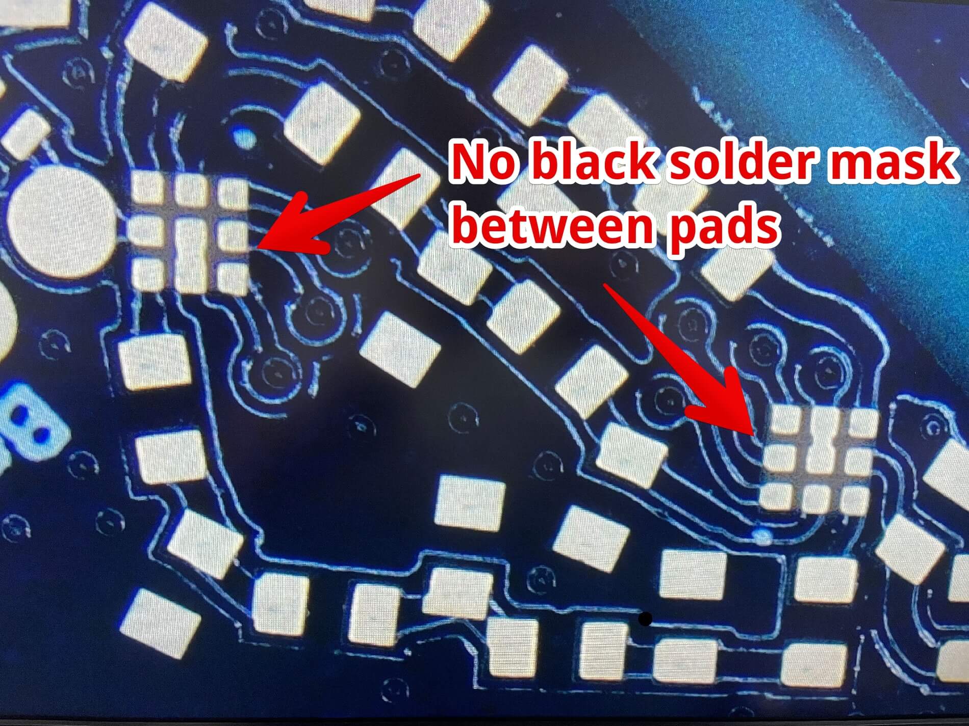
Defective printed circuit board, wrong opening of the mask on the BGA pad. There is no paint between the pads, which increases the risk of sticking contacts when soldering
When the quality of the printed circuit boards meets our requirements, they move on to the next step – assembling the components. The boards are loaded into SMT (Surface Mount Technology), a machine where automatic component placement takes place. This process is also called pick-and-place. The machine grabs the component with a vacuum manipulator and places it on the board.
Setting up the SMT machine, the IR diode on the iButton board is visible on the screen
Boards with installed components are baked in an oven with the appropriate thermal profile. The solder paste is melted and the components are soldered to the board. At this stage, surprises and problems are also possible. If electronic components have not been properly stored and have accumulated moisture inside the case, they may crack at elevated temperatures. Therefore, we order components only from official suppliers who provide a guarantee. This is the only way to get the predicted quality of the final device.
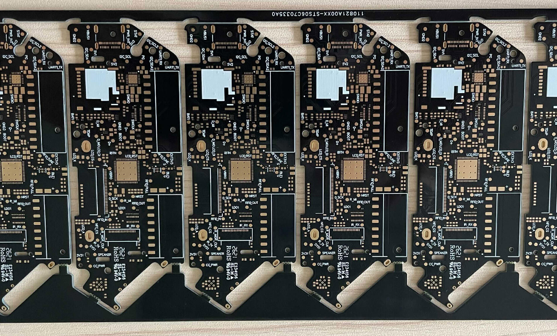
NFC_RFID cards after final assembly of components

Separate NFC_RFID board cut from PCB
After installation, the boards are cut out of the PCB and packed in plastic antistatic trays. At this stage, we do not yet know if these boards work or not. There are probably some defective copies in each batch. Then the batch goes to electrical testing.
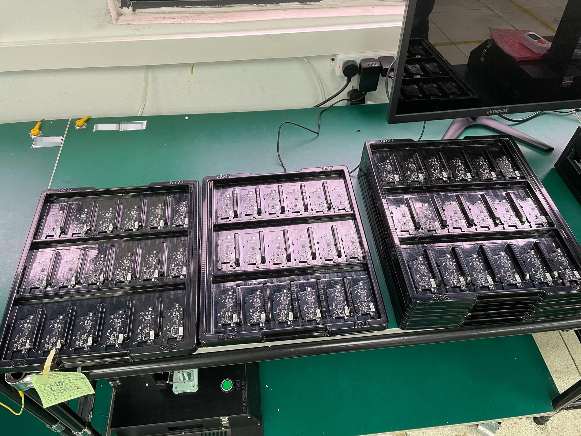
Ready-made NFC boards in anticipation of the first stage of testing

Ready-made NFC boards in anticipation of the first stage of testing

Ready-made iButton boards
What electrical testing looks like
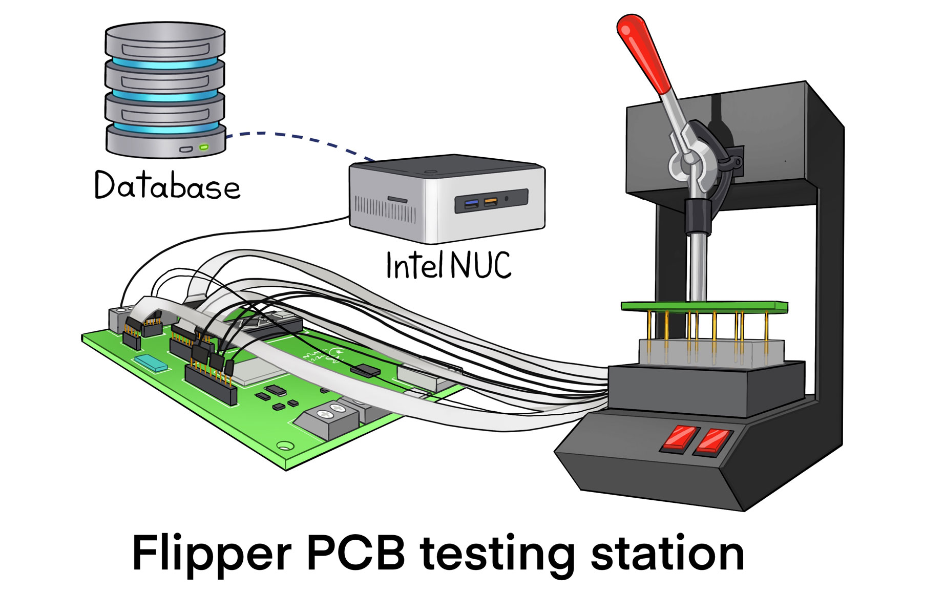
Schematic diagram of the test bench: the needles are connected to the test board, the board is connected to a computer, which uploads the test results to the database
A test bench is developed for each Flipper board, in slang it is called “test jig” or “jig”.
Test jig composition:
- Rigging for a specific board with spring contacts (Bed of nails). Consists of a frame in the shape of a board, a board clamping mechanism (red handle on top).
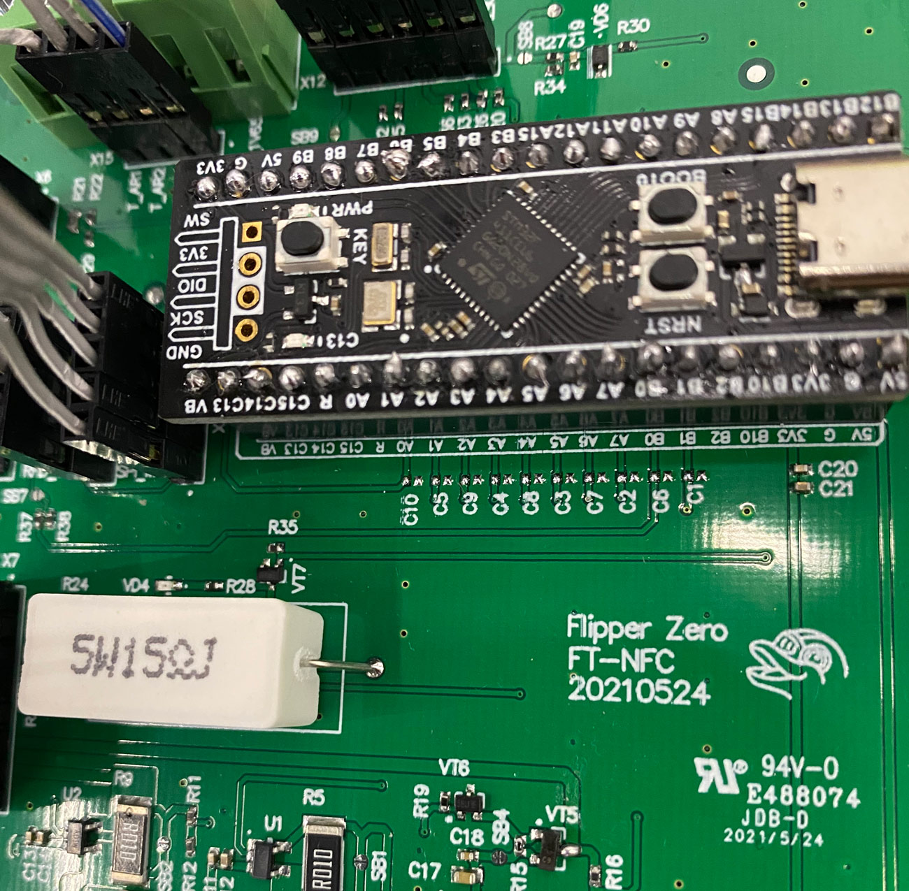
- Control boardto which all spring contacts are connected. We developed this board, as well as the firmware for it, from scratch on the basis of the STM32 microcontroller. For simplicity, a ready-made black pill module on STM32F4 is inserted into the board.
- A computer, which runs the software for testing. The set of tests for each board is different, like the software.
- Databasewhere all test results are sent.
Each Flipper board has its own test station, which contains: a specially designed board for testing, separate firmware for the testing board and software for the computer. This is a huge amount of work, comparable to developing full-fledged devices.

Test stations for all 4 Flipper Zero boards: Main board, NFC + RFID board, iButton + IR board, Antenna board and test station for the device assembly.
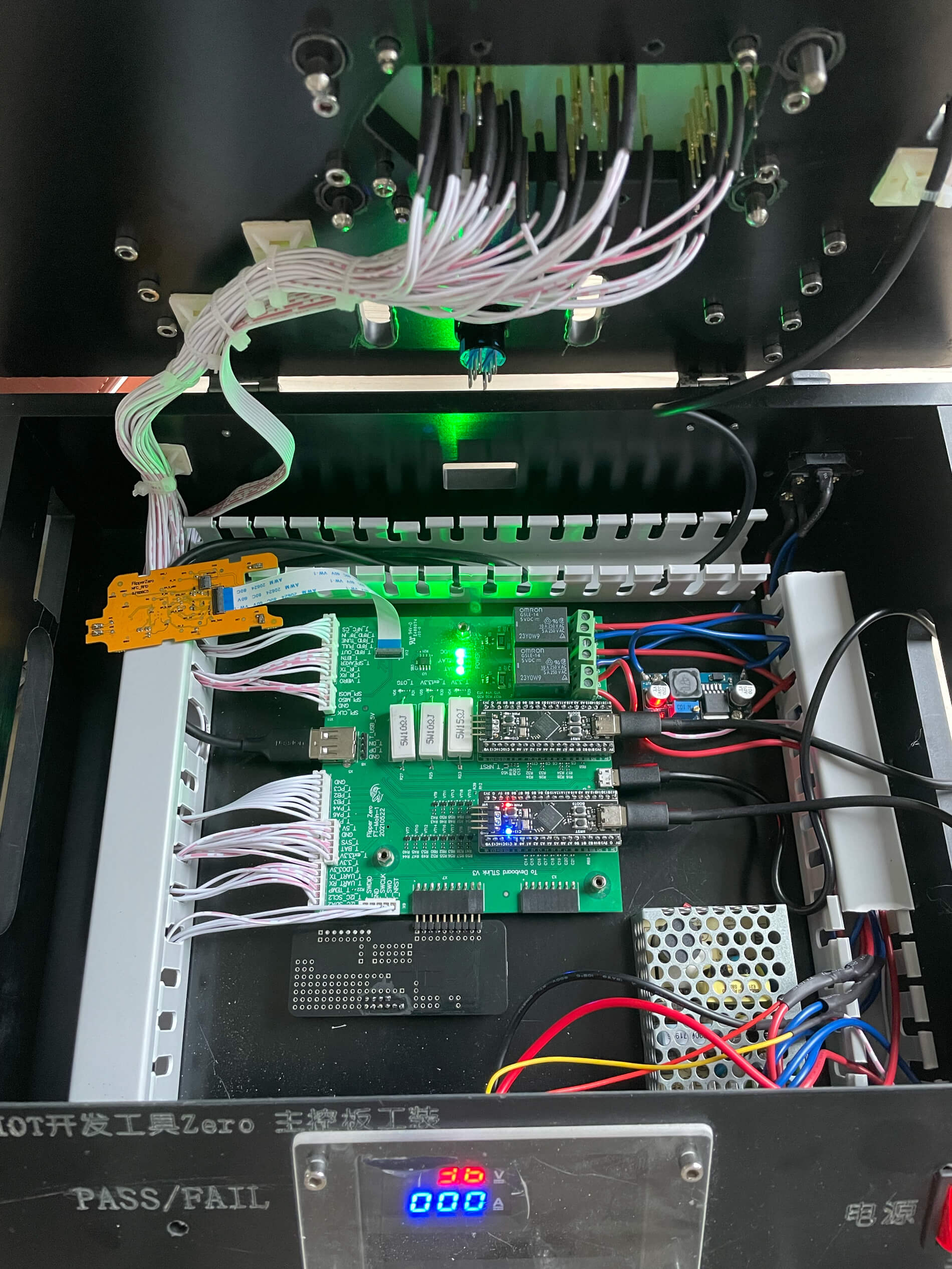
Insides of the test station NFC_RFID
NFC Test Station Board

Testing NFC boards at the stand
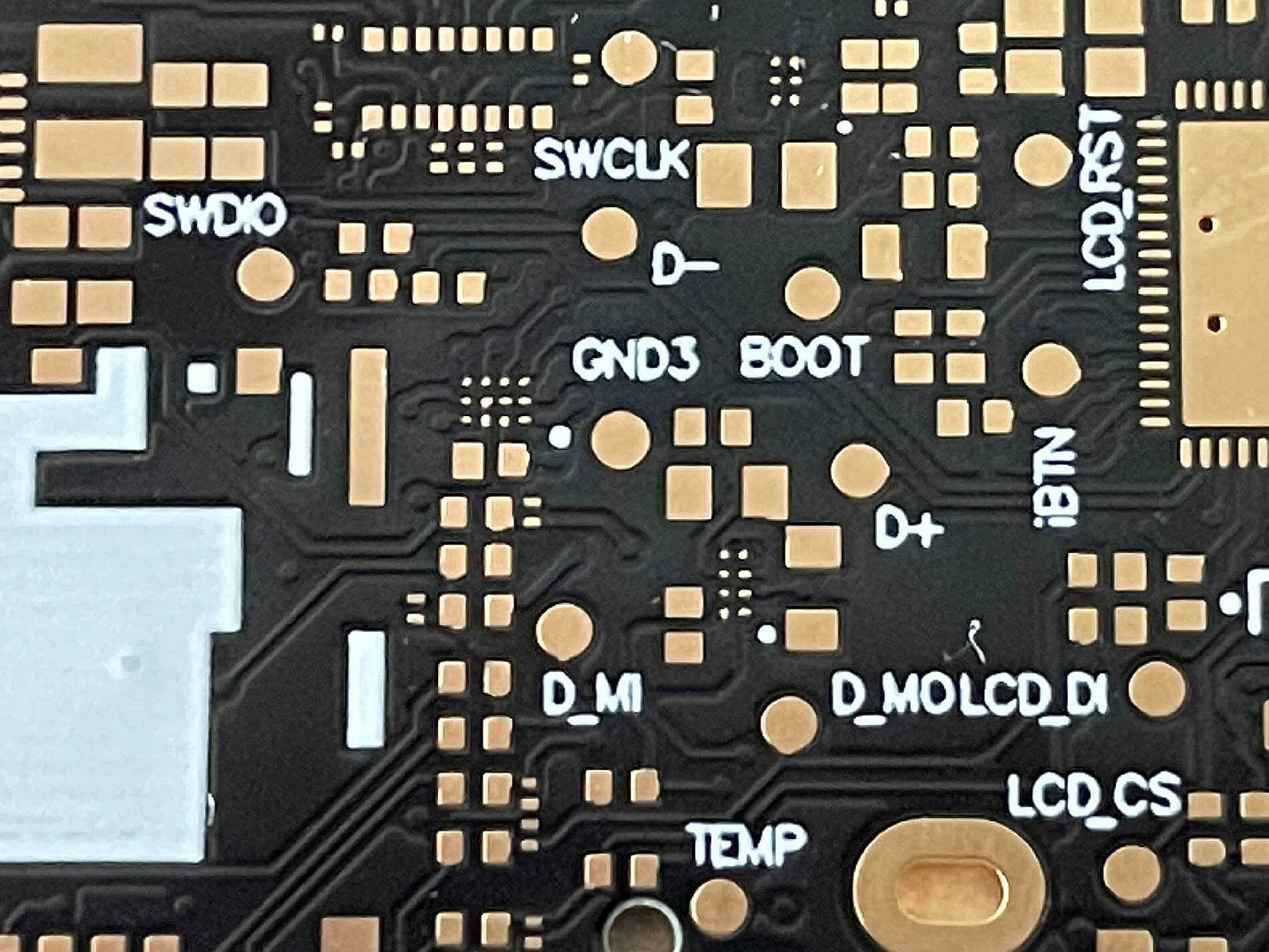
Specially for tests, each Flipper board has test pads where the spring contacts rest. Through them, power is supplied to the device and communication with the electronics on the board takes place.
The testing process looks like this:
1. The board is inserted into the test jig by hand and pressed from above
2. The spring-loaded needles rest against the test pads on the board
3. Automatic tests are run
4. At the exit, the test says PASS or FAIL
5. Everything that has not passed the test goes to the analysis
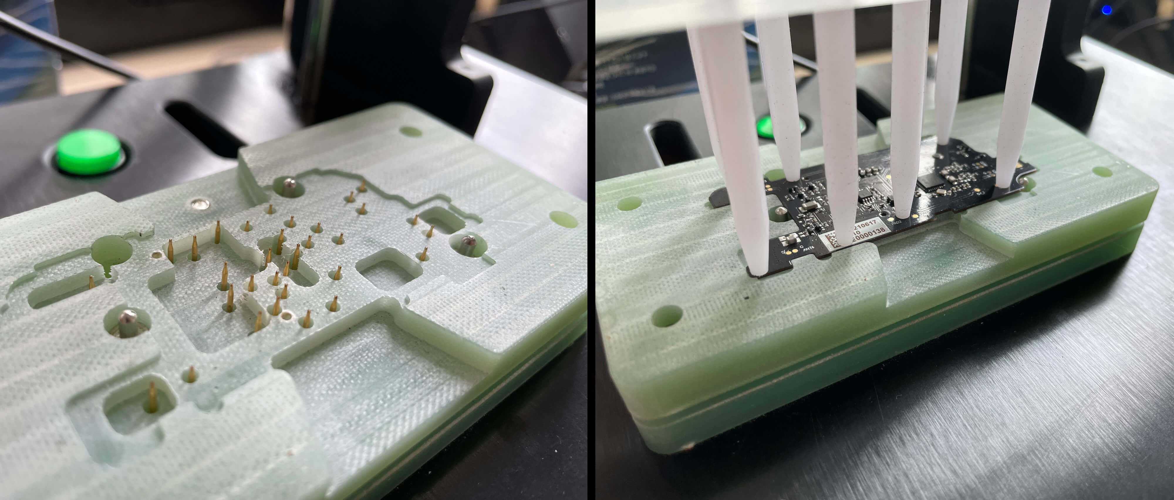
Snap-on for NFC board with spring contacts. The board is clamped in a snap and tests are run.
Video: spring-loaded pins connect to test pads on the board
The test results of each board are saved in a database so that later, by the serial number of the board, one can understand how it passed the tests, when it was produced, and from which batch the components were mounted on it. This is important for looking for any systemic problems.
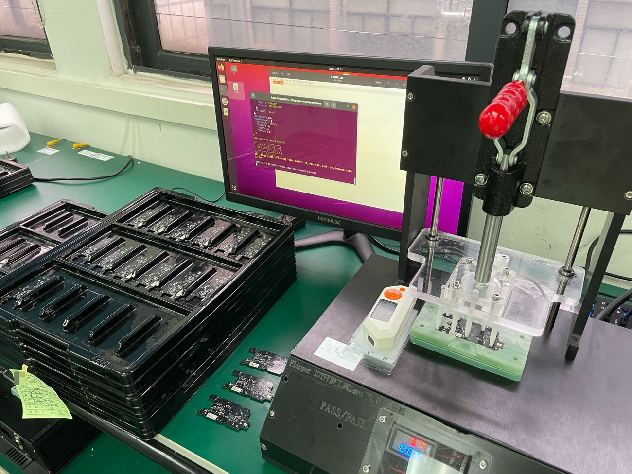
Tester’s workplace
As a result, the actions of the testing operator are reduced to pressing one button and observing the output on the screen. He will see either Pass if the test is successful or Fail. Its task is to set aside defective boards separately.
Successful passing of the test
Why do you need tests of individual boards
Why test each board separately when you can assemble the entire device and then test all the functions already assembled on the finished device?
Assembly is a pipelined process. With smooth production, each next link in the conveyor must check what it gets from the previous one. When there is a systemic defect in the received elements, then it is necessary to investigate the situation and take actions to improve the process at the previous link. If this is not done, then a significant percentage of the assembled devices will have problems of unknown origin.
The defect price found at the stage of the finished product is much higher. Because time has already been spent on the entire production cycle and the final manual assembly of the device. It is more reasonable to localize the problem earlier, on a separate board, and immediately remove the defective board, than to find the problem in the finished device.
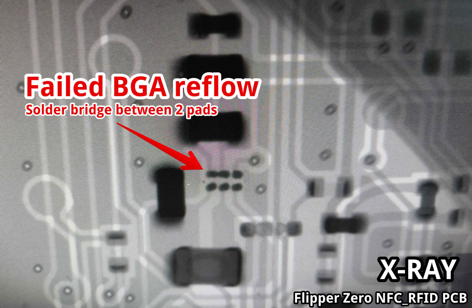
BGA component soldering defect, two points stuck together into one. Revealed by automatic testing.
For example, a real situation: one of the 3 IR diodes was not fully sealed. This problem is immediately caught on the first tests, by the presence of incorrect resistance on the test sites. But if such a board went into a finished device, tests of the finished device as an assembly would show only a low emitted power of the IR transmitter. And then you would have to guess why this happened: problems with connecting loops, problems with power drawdown, etc.
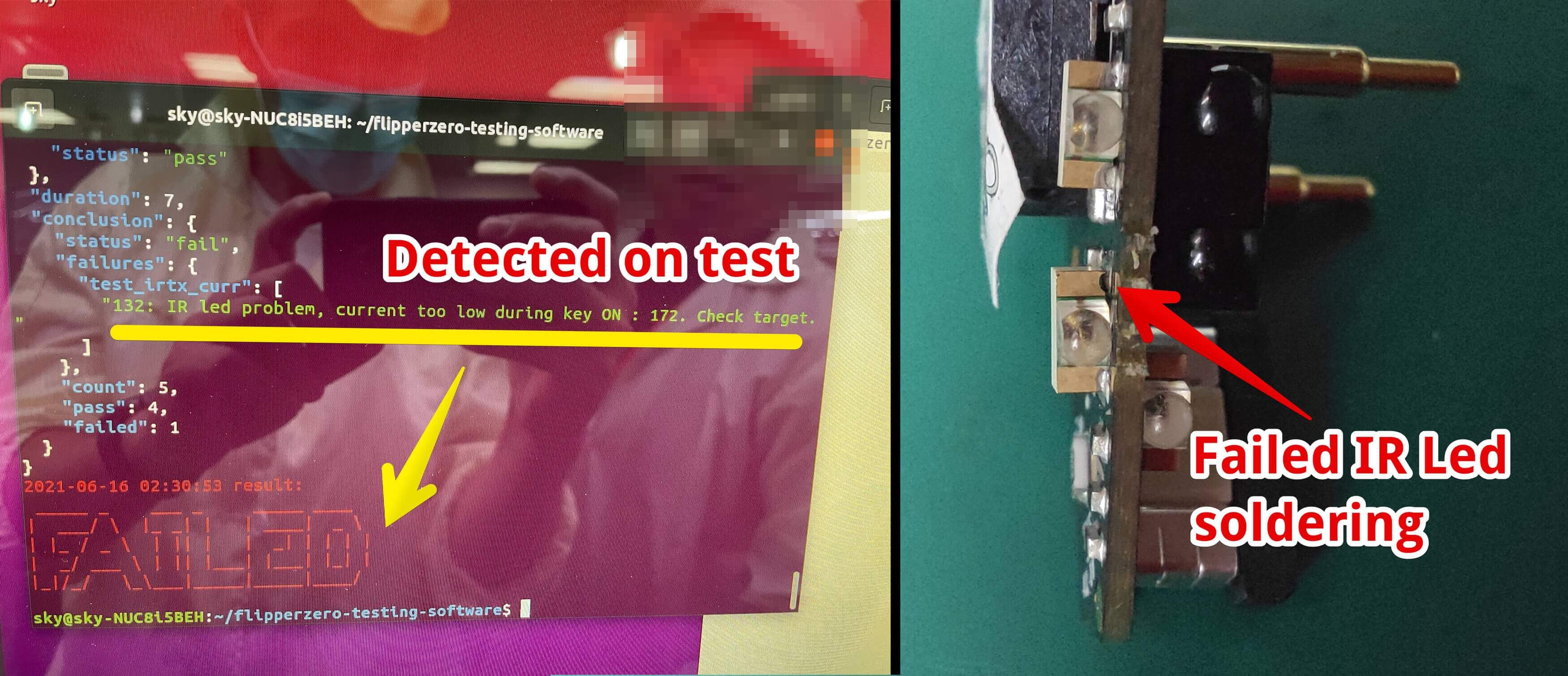
Defect caught in the test – IR diode is not sealed
Sources of test boards
Inside each test station there is a board specially designed for it with its own firmware. We used ready-made Black Pill modules as brains. Below you can see the source code of these boards, through interactive viewer Altium… It contains schematics, the very drawings of the boards and 3D models, right on the habr page!
Main PCB Testing Station
Clickable
NFC_RFID PCB Testing station
Clickable
iButton PCB Testing station
Clickable
Our social networks
 All updates on the project are first published in the Telegeram channel. @zhovner_hub
_________________________________________________________________________________________________________________________________________________________________________________________________________________________________________________________________________________
Pre-order Flipper Zero
The first batch of Flipper Zero has now been launched for backers who ordered the device on Kickstarter. The second batch will be available for purchase in the fall of 2021. You can reserve a device from the second batch in advance here https://shop.flipperzero.one/ This is important for us to more accurately predict production volumes.