Overview of Ultra-Wideband technology based on the DW1000 transceiver (adapter from SPI to UWB)
In this text, I wrote about my experience with UWB. This text will help you understand how to approach UWB transceivers.
There is a DWM1000 module from Decawave (Qorvo). This is a wireless half-duplex transceiver operating at 3.5 GHz to 6.5 GHz with controlled transmission power. It is capable of transmitting data at bit rates up to 6.8Mbit/s

This is the block diagram of the module.

I’ll try to figure out what this chip is capable of.
What do you need from the specifications?
# | doc name | pages | what is there? | Version |
1 | Product Overview | 33 | Module specifications, SoC block diagram, pinout | |
2 | PRODUCT INFORMATION: DWM1000 | 2 | Flyer for DWM1000 module | |
5 | DW1000 USER MANUAL | 249 | Register detail | |
eleven | SOURCES OF ERROR IN DW1000 BASED TWO-WAY RANGING (TWR) SCHEMES | 22 | APS011 APPLICATION NOTE | 1.1 |
9 | DEBUGGING DW1000 BASED PRODUCTS AND SYSTEMS | 23 | APS022 APPLICATION NOTE | 1.3 |
10 | DW1000 DEVICE DRIVER APPLICATION PROGRAMMING INTERFACE (API) GUIDE | 101 | USING API FUNCTIONS TO CONFIGURE AND PROGRAM THE DW1000 UWB TRANSCEIVER | 2.7 |
7 | APS013 APPLICATION NOTE | 15 | The implementation of two-way ranging with the DW1000 | 2.3 |
8 | ANTENNA DELAY CALIBRATION OF DW1000-BASED PRODUCTS AND SYSTEMS | 15 | APS014 APPLICATION NOTE | 1.2 |
3 | PRODUCT BRIEF: DW1000 | 2 | Flyer for DW1000 chip. The name of the pins. | |
4 | Product Overview | 53 | Pinout DW1000 | |
6 | DW1000 Errata | 12 | List of 5 identified chip design bugs |
in the first approximation, inside the DW1000, you can find a PLL, a receive module, a transmitter module, digital logic, an SPI slave, and a power converter.

A more detailed diagram of the DW1000 chip is as follows

Here is the correspondence of the module to its pins

And this is the pinout detail of the DWM1000 module

Inside the DWM1000 is an ASIC called DW1000. Here is a list of his pins.
https://docs.google.com/spreadsheets/d/1ei8rA8kbT_–4zf_2shUHI-hzM8QjJMSJs_8kKTTMak/edit#gid=0
Explicit mapping of 48 pins of the DW1000 chip to 24 pins of the DW moduleM1000 no. As is known from combinatorics, there are 2.000797e+37 ways to orderly select wires 24 out of 48 wires without repetitions. Visually, it is also not clear, since the chip is hidden under the sarcophagus.
To connect the DWM1000 module, I had to make a PCB adapter board
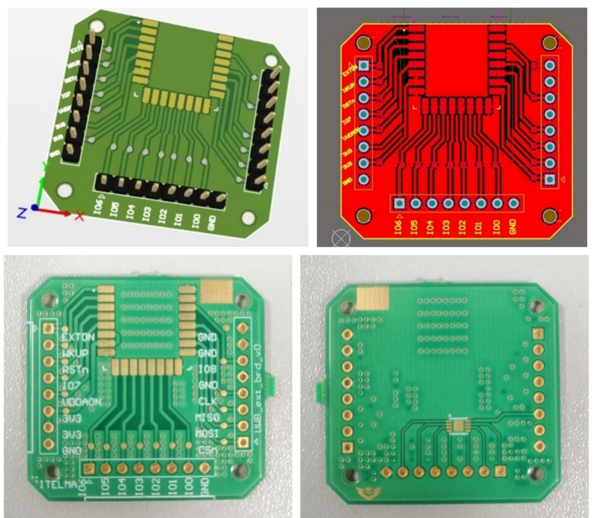
Connection diagram.

The connection diagram is shown here.

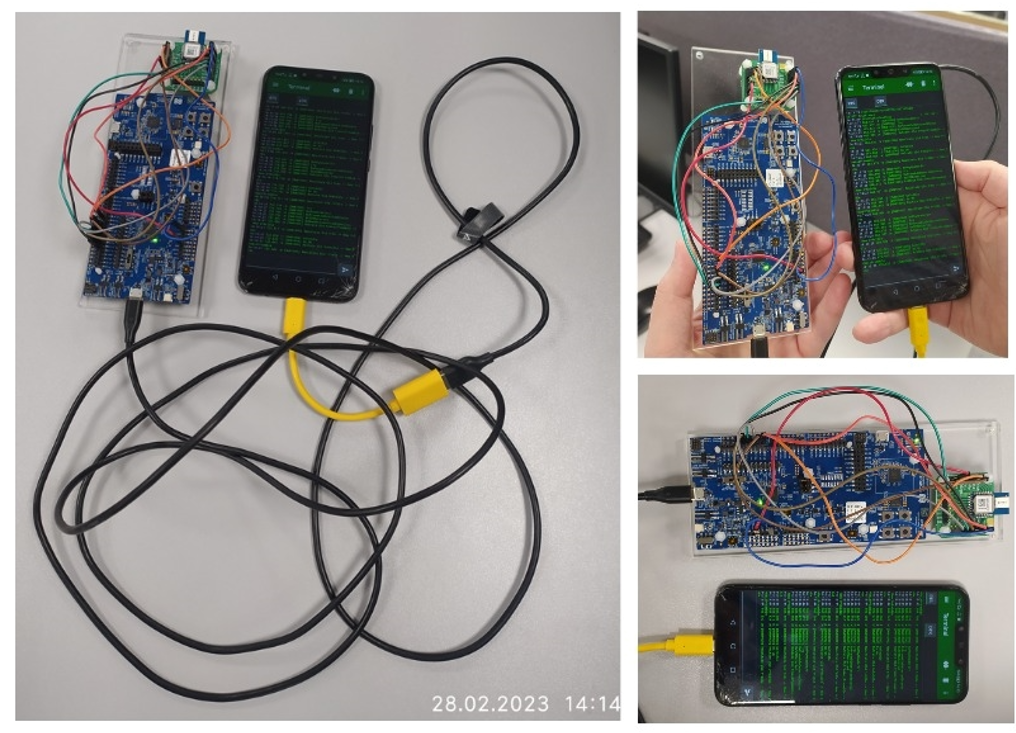
Physically, I had to assemble such a prototype

DWM1000 module control via SPI interface
The QORVO developer company provides its driver for the DW1000 chip. The driver can be downloaded here https://www.qorvo.com/products/p/DW1000#documents. It is enough to download the dw1000_api_rev2p14.zip archive and unpack it. The dw1000_api_rev2p14_stsw\Src folder will contain the C-code of the driver and examples.

There are 101 functions in the original driver. Their list can be viewed here. There is also documentation for the driver in the DW1000 DEVICE DRIVER APPLICATION PROGRAMMING INTERFACE (API) GUIDE dock. It tells you which function is responsible for what.
The chip is fully controlled by the SPI interface. Clock frequency up to 20 MHz. Data is transmitted MSB first. DWM1000 acts as a slave device. The SPI connection parameters are set by selecting the voltage on the GPIO5, GPIO6 pins. By default, they are pulled to the ground. Physically, SPI is full duplex. However, the communication with the device is still half-duplex. The DWM1000 accepts data when the CS wire is 0V. Each negative edge is quoted as the start of a new frame. Therefore, you cannot simply solder the CS to the ground. So the module simply does not understand where the packet begins. Hardware CS won’t work either. We’ll have to do software ChipSelect.

When reading, the DWM1000 sends data low byte first. Therefore, they clearly fall on structures in Little endian processors. Here are the values of the DW1000 registers after correct initialization by the original driver.
+-----+--------------+------+--------+----+----------+
| num |     name     | file | offset |len |   val    |
+-----+--------------+------+--------+----+----------+
|   0 |       DEV_ID | 0x00 | 0x0000 |  4 | 3001CADE | 1101_1110_1100_1010_0000_0001_0011_0000
|   1 |          EUI | 0x01 | 0x0000 |  8 | 00000000FFFFFFFF | ????
|   2 |       PANADR | 0x03 | 0x0000 |  4 | FFFFFFFF | 1111_1111_1111_1111_1111_1111_1111_1111
|   3 |      SYS_CFG | 0x04 | 0x0000 |  4 | 00124000 | 0000_0000_0100_0000_0001_0010_0000_0000
|   4 |     SYS_TIME | 0x06 | 0x0000 |  5 | 00D6C2CE00 | ????
|   5 |     TX_FCTRL | 0x08 | 0x0000 |  5 | 09800A0000 | ????
|   6 |      DX_TIME | 0x0a | 0x0000 |  5 | 0000000000 | ????
|   7 |      RX_FWTO | 0x0c | 0x0000 |  2 |     0000 | 0000_0000_0000_0000
|   8 |     SYS_CTRL | 0x0d | 0x0000 |  4 | 00000000 | 0000_0000_0000_0000_0000_0000_0000_0000
|   9 |     SYS_MASK | 0x0e | 0x0000 |  4 | 00000000 | 0000_0000_0000_0000_0000_0000_0000_0000
|  10 |   SYS_STATUS | 0x0f | 0x0000 |  5 | 0200800000 | ????
|  11 |     RX_FINFO | 0x10 | 0x0000 |  4 | 0980AA10 | 0001_0000_1010_1010_1000_0000_0000_1001
|  12 |     RX_FQUAL | 0x12 | 0x0000 |  8 | 5C001A451031CF2D | ????
|  13 |     RX_TTCKI | 0x13 | 0x0000 |  4 | 0000FC01 | 0000_0001_1111_1100_0000_0000_0000_0000
|  14 |     RX_TTCKO | 0x14 | 0x0000 |  5 | EDFF07391F | ????
|  15 |      RX_TIME | 0x15 | 0x0000 | 14 | 004566DB052CBB3541008066DB05 | ????
|  16 |      TX_TIME | 0x17 | 0x0000 | 10 | 34A6D7B4590066D7B459 | ????
|  17 |      TX_ANTD | 0x18 | 0x0000 |  2 |     3440 | 0100_0000_0011_0100
|  18 |    SYS_STATE | 0x19 | 0x0000 |  4 | 00050540 | 0100_0000_0000_0101_0000_0101_0000_0000
|  19 |   ACK_RESP_T | 0x1a | 0x0000 |  4 | 00000000 | 0000_0000_0000_0000_0000_0000_0000_0000
|  20 |     RX_SNIFF | 0x1d | 0x0000 |  4 | 0000ADDE | 1101_1110_1010_1101_0000_0000_0000_0000
|  21 |     TX_POWER | 0x1e | 0x0000 |  4 | 2202080E | 0000_1110_0000_1000_0000_0010_0010_0010
|  22 |    CHAN_CTRL | 0x1f | 0x0000 |  4 | 22007A4A | 0100_1010_0111_1010_0000_0000_0010_0010
|  23 |    AGC_CTRL1 | 0x23 | 0x0002 |  2 |     01DE | 1101_1110_0000_0001
|  24 |    AGC_TUNE1 | 0x23 | 0x0004 |  2 |     9B88 | 1000_1000_1001_1011
|  25 |    AGC_TUNE2 | 0x23 | 0x000c |  4 | 07A90225 | 0010_0101_0000_0010_1010_1001_0000_0111
|  26 |    AGC_TUNE3 | 0x23 | 0x0012 |  2 |     3500 | 0000_0000_0011_0101
|  27 |    AGC_STAT1 | 0x23 | 0x001e |  3 |   000000 | 0000_0000_0000_0000_0000_0000
|  28 |      EC_CTRL | 0x24 | 0x0000 |  4 | 0400ADDE | 1101_1110_1010_1101_0000_0000_0000_0100
|  29 |      EC_RXTC | 0x24 | 0x0004 |  4 | 00000000 | 0000_0000_0000_0000_0000_0000_0000_0000
|  30 |      EC_GOLP | 0x24 | 0x0008 |  4 | 00DEADDE | 1101_1110_1010_1101_1101_1110_0000_0000
|  31 |    GPIO_MODE | 0x26 | 0x0000 |  4 | 000000DE | 1101_1110_0000_0000_0000_0000_0000_0000
|  32 |     GPIO_DIR | 0x26 | 0x0008 |  4 | FF01ADDE | 1101_1110_1010_1101_0000_0001_1111_1111
|  33 |    GPIO_DOUT | 0x26 | 0x000c |  4 | 000000DE | 1101_1110_0000_0000_0000_0000_0000_0000
|  34 |    GPIO_IRQE | 0x26 | 0x0010 |  4 | 0000ADDE | 1101_1110_1010_1101_0000_0000_0000_0000
|  35 |    GPIO_ISEN | 0x26 | 0x0014 |  4 | 0000ADDE | 1101_1110_1010_1101_0000_0000_0000_0000
|  36 |   GPIO_IMODE | 0x26 | 0x0018 |  4 | 0000ADDE | 1101_1110_1010_1101_0000_0000_0000_0000
|  37 |    GPIO_IBES | 0x26 | 0x001c |  4 | 0000ADDE | 1101_1110_1010_1101_0000_0000_0000_0000
|  38 |    GPIO_ICLR | 0x26 | 0x0020 |  4 | 0000ADDE | 1101_1110_1010_1101_0000_0000_0000_0000
|  39 |    GPIO_IDBE | 0x26 | 0x0024 |  4 | 0000ADDE | 1101_1110_1010_1101_0000_0000_0000_0000
|  40 |     GPIO_RAW | 0x26 | 0x0028 |  4 | 000000DE | 1101_1110_0000_0000_0000_0000_0000_0000
|  41 |   DRX_TUNE0b | 0x27 | 0x0002 |  2 |     1600 | 0000_0000_0001_0110
|  42 |   DRX_TUNE1a | 0x27 | 0x0004 |  2 |     8D00 | 0000_0000_1000_1101
|  43 |   DRX_TUNE1b | 0x27 | 0x0006 |  2 |     6400 | 0000_0000_0110_0100
|  44 |    DRX_TUNE2 | 0x27 | 0x0008 |  4 | 5E013B35 | 0011_0101_0011_1011_0000_0001_0101_1110
|  45 |   DRX_SFDTOC | 0x27 | 0x0020 |  2 |     4110 | 0001_0000_0100_0001
|  46 |   DRX_PRETOC | 0x27 | 0x0024 |  2 |     0000 | 0000_0000_0000_0000
|  47 |   DRX_TUNE4H | 0x27 | 0x0026 |  2 |     2800 | 0000_0000_0010_1000
|  48 |  DRX_CAR_INT | 0x27 | 0x0028 |  3 |   000000 | 0000_0000_0000_0000_0000_0000
|  49 | RXPACC_NOSAT | 0x27 | 0x002c |  2 |     0000 | 0000_0000_0000_0000
|  50 |      RF_CONF | 0x28 | 0x0000 |  4 | 00000000 | 0000_0000_0000_0000_0000_0000_0000_0000
|  51 |   RF_RXCTRLH | 0x28 | 0x000b |  1 |       D8 | 1101_1000
|  52 |    RF_TXCTRL | 0x28 | 0x000c |  3 |   A05C04 | 0000_0100_0101_1100_1010_0000
|  53 |    RF_STATUS | 0x28 | 0x002c |  4 | 09DEADDE | 1101_1110_1010_1101_1101_1110_0000_1001
|  54 |      LDOTUNE | 0x28 | 0x0030 |  5 | 8888888808 | ????
|  55 |      TC_SARC | 0x2a | 0x0000 |  2 |     0000 | 0000_0000_0000_0000
|  56 |      TC_SARL | 0x2a | 0x0003 |  3 |   000000 | 0000_0000_0000_0000_0000_0000
|  57 |      TC_SARW | 0x2a | 0x0006 |  2 |     0000 | 0000_0000_0000_0000
|  58 |   TC_PG_CTRL | 0x2a | 0x0008 |  1 |       BC | 1011_1100
|  59 | TC_PG_STATUS | 0x2a | 0x0009 |  2 |     F90B | 0000_1011_1111_1001
|  60 |   TC_PGDELAY | 0x2a | 0x000b |  1 |       C5 | 1100_0101
|  61 |    TC_PGTEST | 0x2a | 0x000c |  1 |       00 | 0000_0000
|  62 |    FS_PLLCFG | 0x2b | 0x0007 |  4 | 08054008 | 0000_1000_0100_0000_0000_0101_0000_1000
|  63 |   FS_PLLTUNE | 0x2b | 0x000b |  1 |       26 | 0010_0110
|  64 |     FS_XTALT | 0x2b | 0x000e |  1 |       72 | 0111_0010
|  65 |     AON_WCFG | 0x2c | 0x0000 |  2 |     2000 | 0000_0000_0010_0000
|  66 |     AON_CTRL | 0x2c | 0x0002 |  1 |       00 | 0000_0000
|  67 |     AON_RDAT | 0x2c | 0x0003 |  1 |       00 | 0000_0000
|  68 |     AON_ADDR | 0x2c | 0x0004 |  1 |       00 | 0000_0000
|  69 |     AON_CFG0 | 0x2c | 0x0006 |  4 | EE1FFF50 | 0101_0000_1111_1111_0001_1111_1110_1110
|  70 |     AON_CFG1 | 0x2c | 0x000a |  2 |     0000 | 0000_0000_0000_0000
|  71 |     OTP_WDAT | 0x2d | 0x0000 |  4 | 00000000 | 0000_0000_0000_0000_0000_0000_0000_0000
|  72 |     OTP_ADDR | 0x2d | 0x0004 |  2 |     1E00 | 0000_0000_0001_1110
|  73 |     OTP_CTRL | 0x2d | 0x0006 |  2 |     0000 | 0000_0000_0000_0000
|  74 |     OTP_STAT | 0x2d | 0x0008 |  2 |     0000 | 0000_0000_0000_0000
|  75 |     OTP_RDAT | 0x2d | 0x000a |  4 | 12010000 | 0000_0000_0000_0000_0000_0001_0001_0010
|  76 |    OTP_SRDAT | 0x2d | 0x000e |  4 | 00000000 | 0000_0000_0000_0000_0000_0000_0000_0000
|  77 |       OTP_SF | 0x2d | 0x0012 |  1 |       00 | 0000_0000
|  78 |   LDE_THRESH | 0x2e | 0x0000 |  2 |     0000 | 0000_0000_0000_0000
|  79 |     LDE_CFG1 | 0x2e | 0x0806 |  1 |       00 | 0000_0000
|  80 |   LDE_PPINDX | 0x2e | 0x1000 |  2 |     0000 | 0000_0000_0000_0000
|  81 |   LDE_PPAMPL | 0x2e | 0x1002 |  2 |     0000 | 0000_0000_0000_0000
|  82 |   LDE_RXANTD | 0x2e | 0x1804 |  2 |     0000 | 0000_0000_0000_0000
|  83 |     LDE_CFG2 | 0x2e | 0x1806 |  2 |     0000 | 0000_0000_0000_0000
|  84 |     LDE_REPC | 0x2e | 0x2804 |  2 |     0000 | 0000_0000_0000_0000
|  85 |     EVC_CTRL | 0x2f | 0x0000 |  4 | 00DEADDE | 1101_1110_1010_1101_1101_1110_0000_0000
|  86 |      EVC_PHE | 0x2f | 0x0004 |  2 |     0000 | 0000_0000_0000_0000
|  87 |      EVC_RSE | 0x2f | 0x0006 |  2 |     0000 | 0000_0000_0000_0000
|  88 |      EVC_FCG | 0x2f | 0x0008 |  2 |     0000 | 0000_0000_0000_0000
|  89 |      EVC_FCE | 0x2f | 0x000a |  2 |     0000 | 0000_0000_0000_0000
|  90 |      EVC_FFR | 0x2f | 0x000c |  2 |     0000 | 0000_0000_0000_0000
|  91 |      EVC_OVR | 0x2f | 0x000e |  2 |     0000 | 0000_0000_0000_0000
|  92 |      EVC_STO | 0x2f | 0x0010 |  2 |     0000 | 0000_0000_0000_0000
|  93 |      EVC_PTO | 0x2f | 0x0012 |  2 |     0000 | 0000_0000_0000_0000
|  94 |     EVC_FWTO | 0x2f | 0x0014 |  2 |     0000 | 0000_0000_0000_0000
|  95 |     EVC_TXFS | 0x2f | 0x0016 |  2 |     0000 | 0000_0000_0000_0000
|  96 |      EVC_HPW | 0x2f | 0x0018 |  2 |     0000 | 0000_0000_0000_0000
|  97 |      EVC_TPW | 0x2f | 0x001a |  2 |     0000 | 0000_0000_0000_0000
|  98 |     DIAG_TMC | 0x2f | 0x0024 |  2 |     0000 | 0000_0000_0000_0000
|  99 |   PMSC_CTRL0 | 0x36 | 0x0000 |  4 | 000230F0 | 1111_0000_0011_0000_0000_0010_0000_0000
| 100 |   PMSC_CTRL1 | 0x36 | 0x0004 |  4 | 38070281 | 1000_0001_0000_0010_0000_0111_0011_1000
| 101 |   PMSC_SNOZT | 0x36 | 0x000c |  1 |       40 | 0100_0000
| 102 |  PMSC_TXFSEQ | 0x36 | 0x0026 |  2 |     740B | 0000_1011_0111_0100
| 103 |    PMSC_LEDC | 0x36 | 0x0028 |  4 | 200000DE | 1101_1110_0000_0000_0000_0000_0010_0000
+-----+--------------+------+--------+----+----------+
the transceiver can be in the following states
No. | State | Description |
1 | OFF | chip without power |
10 | WAKEUP | Quartz included. LDO enabled. |
2 | powerup | — |
8 | DEEPSLEEP | SPI transmission not possible |
3 | INIT | Quartz works. SPI can only work at 3MHz |
4 | IDLE | PLL included. SPI can run at full speed 20MHz |
6 | TX | The transceiver transmits a packet. Then it will switch to IDLE. |
7 | RX PREAMBLE SNIFF | The transceiver periodically switches between IDLE and RX |
5 | RX | The transceiver is looking for a preamble |
8 | SLEEP | SPI transmission is not possible. Consumption is less than 1uA. LDOs are off. |
9 | SNOOZE | — |
Own SPI registers of the DW1000 chip
Register files are addressed with 6 bits. This means that 64 register files can be addressed. It has 110 registers in total.
https://docs.google.com/spreadsheets/d/1-cDqzBLOIxD7zWVG7oPmD_uq-V_fILkTvu4ADGFD_5E/edit#gid=0
What settings should be assigned in the DWM1000 chip?
Parameter | Units | parameter type |
TxPower | dBm | main |
preamble length | Symbols | derivative |
Receive channel | num | derivative |
preamble code | ? | derivative |
channel | main | |
transmission channel | num | derivative |
bandwidth | Hz | derivative |
center frequency | Hz | derivative |
bit rate | bit/s | main |
Transmit Pulse Repetition Frequency | Hz | main |
The channel number completely defines the center frequency, channel width and preamble code. The channel number of the transmitter and the channel number of the receiver must always match in each individual transceiver.

Here is the parameter dependency tree

What parameters affect the radio range?
The bit rate and preamble length affect the range. The longer preamble provides improved range. When the bit rate is high, the operating range is short. At a low bit rate, data can be transmitted over long distances.
Radio Packet Format
A radio packet consists of a preamble, a start frame delimiter, a header, and a payload.

The DW1000 has a hardware 40-bit timer. It can count from 0 to 2^40=1 099 511 627 776. This timer is clocked at 64 GHz. This means that it overflows every 17.17 seconds. This timer is incremented by 1 every 15.625ps. Light during this time manages to pass 0.004m or 4mm.
The chip inserts a timestamp between the SFD and PHR fields. This timestamp can be read from register 0x15.
Data transfer

Data reception

Since UWB is a technology for mobile technology, we had to debug it by connecting to a smartphone via Serial Over USB using the iconic Android application Serial USB Terminal.

This is what the debug kit looked like
DW1000 Chip Calibration
If you read the TimeStamp(s) values from the registers immediately after initialization, then the values will not be valid. You will get 120…160 meters between transceivers when the distance is only one and a half meters. This is due to the floating parameters in the manufacture of silicon wafers.
Calibration parameters are written to OTP memory. The microcontroller can read data from the OTP and write it to the DW1000 registers.
To calibrate the antenna delay, you need to take two DW1000s, set them to a known distance and measure the range. The antenna delay is adjusted until the actual range and the read range start to match. Then the antenna delay value should be written to the OTP memory. There is a delay in sending and a delay in receiving.
Send latency is the time between the internal digital timestamp and the actual time of sending to the antenna.
The receive lag is used to compensate for the time between the reception of the RMARKER signal in the antenna and the internal time stamp in the digital circuit.
In many implementations of the PCB, the receive and send latencies are equal.
Link(s) radio range test
Indoors, I spaced two DW1000 transceivers 24 paces (16.5m) and the UWB packets consistently arrived in both directions. Further interfered with the geometry of the room. On the street, I was able to receive ping at a distance of 76 meters.
SS-TWR/DS-TWR Ranging Testing
Testing of ranging technology without calibration shows that with a distance between transceivers of only 0.89m, measurements show values of the order of 154.6 meters. Moreover, the spread was 0.9 meters.

Project ideas for UWB transceivers
UWB chat. Instant text messaging.
Firmware update by radio
Transferring files by radio
InDoor navigation
Remote control of electronic devices in the room
Dictionary
To work with the DWM1000, you need to understand the following acronyms
Acronym | Decryption |
AON | Always On |
POR | Power On Reset |
API | Application Programming Interface |
ETSI | European Telecommunications Standards Institute |
N.B. (N.B.) | Nota bene (note well) |
PAC | preamble acquisition chunk |
SFD | start of frame delimiter |
DW | DecaWave |
XTI | internal 19.2 MHz clock (is the raw 38.4 MHz XTAL oscillator input ÷ 2) |
PRF | pulse repetition frequency |
BPM | bi-phase modulation |
ISO | International Organization for Standardization |
BPSK | binary phase shift keying |
MSB | most significant bit |
FCS | Frame Checking Sequence |
TWR | two way ranking |
LO | local oscillator |
IEEE | Institute of Electrical and Electronic Engineers |
PLL | Phase Locked Loop |
CS | chip select. |
CMOS | Complementary metal-oxide-semiconductor |
QFN | quad-flat no-leads |
LSB | Least Significant Bit |
LDE | leading edge (or the process to find and adjust the RX message timestamp) |
LED | light emitting diode |
PHR | PHY header |
PHY | physical layer |
SPI | Serial Peripheral Interface |
GPIO | General Purpose Input Output |
OTP | One Time Programmable |
RTLS | real time location systems |
WSNs | wireless sensor networks |
RST | reset |
TOF | time of flight |
IC | integrated circuit |
FCC | Federal Communications Commission |
TDOA | Time Difference of Arrival |
MAC | Media Access Control |
CRC | cyclic redundancy check |
UWB | ultra wideband |
TWR | two way ranging |
TX | transmit |
RF | radio frequency |
PSD | power spectral density |
EIRP | Effective Isotropic Radiated Power |
PCB | printed circuit board |
FEC | forward error correction |
Conclusion
The DW1000 itself is very crude. To simply set up a channel, you need to write magic numbers into a dozen registers. In this case, part of the registers are addressed by 2 bytes, and part by 3 bytes. Although there are only 110 registers. The registers themselves are torn, of different sizes. To write OTP parameters, you need a voltage slightly higher than the usual 3.3V per VCC (3.8V). RxTimeStamp must be enabled separately. Antenna delay calibration is required.
There are many registers. The dw1000 chip requires a relatively complex driver. It makes no sense to write your own driver for it. It is better to take the driver from the vendor. Data was transmitted in both directions at distances up to 78 meters. Determine Tx TimeStamp(s). At first glance, the range is determined with an accuracy of + – 45cm. In general, the dw1000 chip is complex.
Another module can be used as a GPIO expander. From SPI to 8 pins.
As for me, Duck UWB is an excellent interface for updating the firmware or for remote control, but in order to measure the range, you need to build a calibration bench 10 meters in size.
Links
Documentation about the module
Documentation about the DW1000 chip: