Mapper – ours, or another technology for electron-multi-beam lithography
Previous Article – Technology from IMS Nanofabrication
The technology from IMS, briefly described in the previous article, does not have enough performance to compete in the mass-produced chip market. It is good for the production of photomasks, as well as prototypes and small batches. exclude such an expensive link as photomasks (masks).
However, at about the same time, when in Austria they designed their installation at IMS, in the Netherlands they also decided to try their hand at this direction.
Moreover, we set ourselves the task of achieving a productivity of at least 10 pieces per hour for 300 mm plates.
MAPPER- acronym stands for Multra Aperture Pixel by Pixel Enhancement of Resolution, i.e. multi-aperture pixel-by-pixel resolution enhancement. The name of the technology has almost nothing to do with its essence.

The foundation was laid in 1998 by Pieter Kruit from the Technische Universiteit Delft, TU Delft, in the Netherlands. A little later Bert Jan Kampherbeek and Marco Wieland joined him. To commercialize the technology, a small start-up called Mapper Lithography was created in 2000. The university became one of the shareholders.
In 2001, one of the first investors was Arthur del Prado, founder of ASM and ASML.
In 2008, two laboratory prototype devices were built.
Since 2010, funding for development under the European MAGIC program has begun (MAskless lithoGraphy for IC manufacturing), 11.75 million euros were allocated to support MAPPER and IMS Nanofabrication.
In 2012, 40 million euros were invested in the creation of production in the Netherlands, in the same year cooperation with the Rosnano corporation began, which allocated another 40 million euros (1 billion rubles) to create the production of MEMS electronic-optical elements (a key link in technologies), and one of the conditions was the location of the enterprise in Russia. 2014 launch of production in Russia.
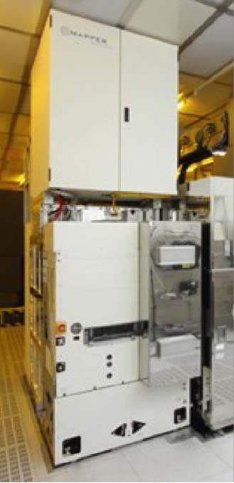
In 2015, the first sample of an industrial lithograph (FLX-1200) was assembled, capable of recording 1 piece / hour of 300mm plates at a technological standard of 28nm.
September 9, 2016 is the worst day in Mapper’s history. On this day, the main investor Arthur del Prado died. This man is a legend in the world of microelectronic lithography. A man with the rare ability to see the future. You can say the founding father
of European microelectronics, which made its company ASML the most important link in the entire world microelectronics industry.


But back to Mapper.
Since 2017, the FLX-1200 lithograph has been available as a demo.
In 2018, the 2nd sample was assembled, but investments in the company were stopped and in December of the same year the company was declared bankrupt.
In January 2019, AMSL, as the most interested, won the Mapper Lithography auction.
All intellectual property has been transferred to ASML. Although AMSL does not announce any news about the work on the technology, non-AMSL entities in the PRC are believed to be working on the technology.

The flow of electrons diverging from the electron source, having passed through the collimator macro-lens (Collimator lens) in the form of a parallel stream falls on an array of aperture holes (Apertute array). The holes form a beam of >13’000 rays. Each beam using an array of condenser micro-lenses (Condensor lens array) is focused into the centers of the holes of the beam-blanking array (Beam blanker array).
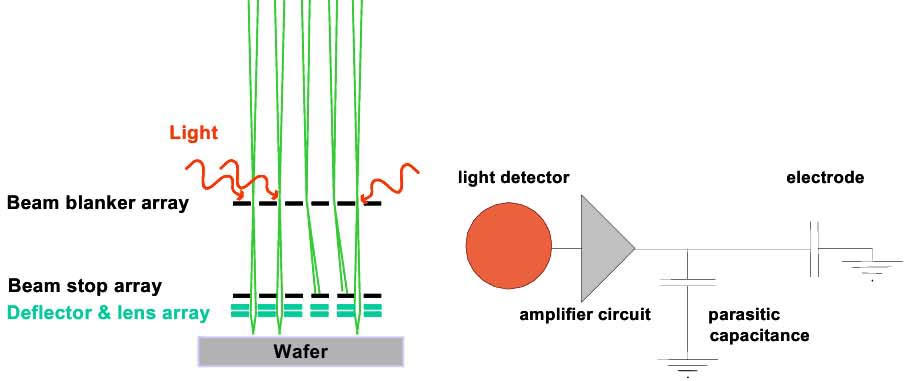
This array, made using CMOS and MEMS technology, included photodiode elements that received control light (Light) from a laser system. This decision is explained by the data rate (7.6 Gbit/s per microcolumn). Extinguishable beams are discarded to the Beam stop array. Beams that weren’t discarded go through the Beam stop array and end up in the array micro-columns consisting of an array of deflectors and lenses (Deflector & lens array). Each micro-the lens in the array focuses a single beam on the plate and deflects in the 2 µm range at a frequency of 6 MHz and an accuracy of 1 nm. The beams are deflected simultaneously in all micro-lenses.
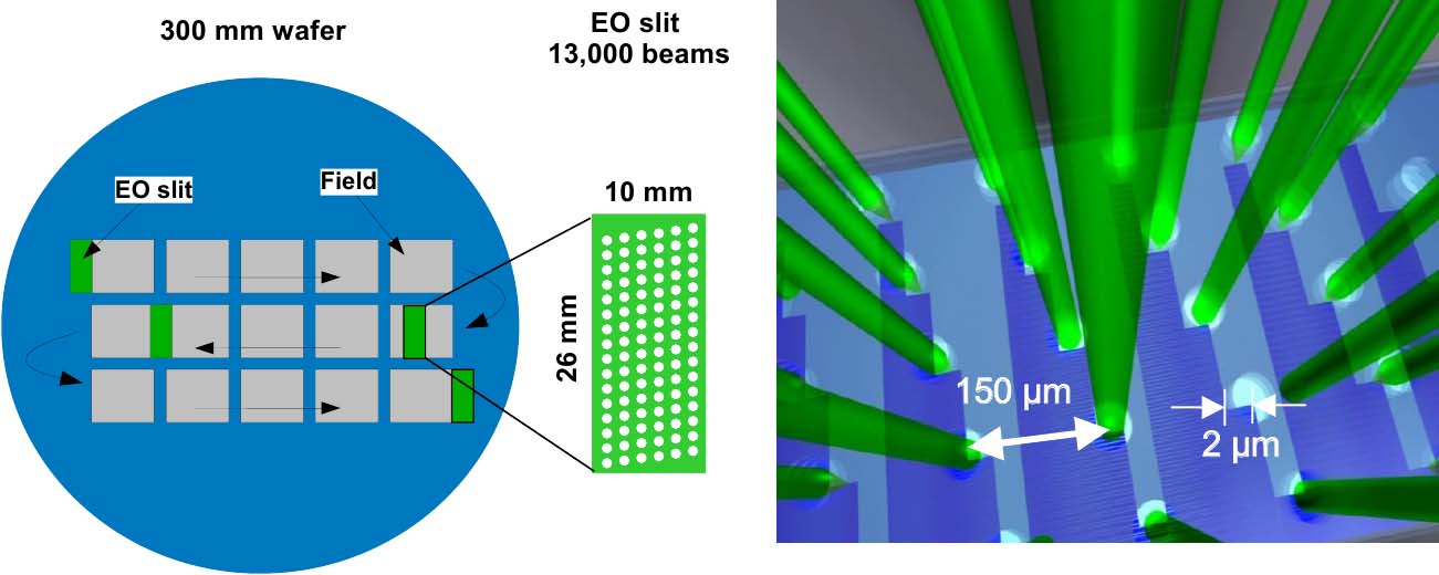
In the first Mappers, the array of rays was formed from 13’050 rays (174×75) rays in a rectangle 26.1×11.25 mm. This made it possible to illuminate a rectangle that approximately corresponds to the “standard” field of 26×33 mm in projection lithography, illuminated in one step of the stepper (with a mask of 104×132 mm at 4x reduction).
In the direction of 26 mm, the step of the beams is 150 μm, in the direction of 10 mm, the step between the rows is also 150 μm, and each subsequent row is shifted relative to the previous one by 2 μm. Recording proceeds in the direction perpendicular to the wide side (26 mm).

1 – source, 3 – collimator electrostatic macro-lens, 4 – aperture plate, 5 – system of electrostatic focusing micro-lenses (MEMS plate), 6 – aperture plate forming sub-beams (groups 7×7), 7 – control system (blanker ), an array of MEMS deflector electrodes that deflect sub-beams, 8 – a MEMS quenching plate, an array of aperture holes through which sub-beams not deflected by the control plate pass, beams, 10 – focusing system that produces the final focusing on the target surface (MEMS plate), 11 – target (silicon plate), 16 – coordinate table, 20 – divergent electron flow, 21 – collimated electron beam, 22 – main electron beams (1352 pcs.), 23 – sub-beams (66’248 pcs., in groups of 49 pcs.), 24 – reduced beams that form the final pattern, 140 – control system.
Subsequently, in the FLX-1200 demo sample, the number of beams was increased to 66’248 pieces, divided into groups of 49 (7×7) beams. First, the total collimated electron flow was divided into 1352 “thick” beams, then each “thick” beam was divided into 49 sub-beams. Moreover, the configuration of the matrix of rays was changed – between the fields of sub-beams, “passages” were allocated for laser beams that control the matrix. Each laser beam controlled a group of sub-beams. Laser beams were emitted from the ends of the optical fibers and focused on receivers located between the rows. The entire system was controlled via 888 fibers.
The stated goal of 10 pieces/hour of 300 mm wafers required a total current on the wafer surface of the order of 150 μA. If you use an accelerating voltage of 100 kV, then 15 W will be released on the plate – this is unacceptable, so the accelerating voltage is reduced to 5 kV, which gives 0.75 W on the plate at a current of 150 μA.
However, a current of 150 µA on the plate for an electron source used on a MAPPER column with a brightness of about 10^6 A / (cm2 * sr * V), taking into account the losses on the aperture plate, which passes only a small fraction of the total flow, is actually unattainable.
So on a demonstration industrial sample, the current of a single beam in micro-column 0.26 nA, thus, with the number of rays 66’248pcs. the total current incident on the plate was ~17 μA.
At the same time, the productivity reached only 1 piece/hour of 300 mm wafers at a technological standard of 28 nm. Although this is a fairly high performance, it is only 1/10 of the target.
In the future, to improve performance, it was planned to use a source with a lower brightness (dispenser cathode), but a higher current. For multibeam lithography with a spot of 20 nm, this is quite acceptable. Although, in this case, the cathode itself would become an additional source of contamination in the optical system. You will also have to take care of cooling the first aperture plate and the collimator lens – the details that perceive most of the radiation.
A rather technically complicated concept of beam separation according to micro-columns was chosen to eliminate the Coulomb repulsion forces of similarly charged particles. Because quite a lot of current is required for target performance, it becomes impossible to use the crossover (point of convergence of all beams) used in cathode beam optics to focus the beam and reduce the spot size. Managing thousands micro-columns require a rather complex electronic part and precision manufacturing of the micro-colon. To do this, with the financing of Rosnano, their own production was created in Moscow (LLC Mapper, mapperllc.ru). Although Mapper’s equipment is standard in the industry, its configuration is unusual for a MEMS company. This is due to the strict requirements for the production of micro-lens electronic optics.
But, the problems of unstable operation of the electron source at high currents, and in the control micro-columns, allowed to achieve only 1/10 of the target performance.
Apparently, with the death of the main investor, Artur del Prado, the confidence of the rest melted away, and their patience ran out.
Previous Article – Technology from IMS Nanofabrication


