Connecting the TM1638 module to Arduino without the SPI library
Initially, the task was stated as follows. I had a TM1638 board available. It was necessary to learn how to work with it (well, and check the functionality of the board itself) in order to use it in one interesting project (more on that another time). I had an Arduino Nano handkerchief at hand. I wanted it quickly get off I couldn’t check the operation of the board itself using the Arduino SPI.h library. As a result, the amount of work done resulted in this note.

Let me start by saying that I bought this board to complete tasks Schools of Synthesis. And when I ordered, I didn’t look at what it was (the School has ready-made scripts for connecting hardware, which is very convenient when starting training from scratch). When it arrived, I realized that I couldn’t connect it without scripts, because it has an SPI interface, and I had never worked with it before, even in microcontrollers (I don’t know how it happened that it bypassed me).
Therefore, I decided to describe the entire work process, in case it will be useful to someone.
In the classic version, SPI uses four wires for transmission: SCLK for transmitting the clock signal, MOSI and MISO for transmitting data from the master (master) to the slave and back, and SS for selecting the slave. You can read more about SPI itself and about connecting devices to the bus on the Internet (for example, here described, in my opinion, well and with pictures).
The TM1638 module has five pins, two of them are ground and power, but the other three are for data exchange. One to send it the clock signal from the master (CLK), one to control the transfer process (STB) and one to transfer the data itself (DIO). Those. This SPI implementation is half-duplex – the same wire is used to transmit and receive data.
There are several commands to control the module: brightness control (and on/off) (Display Control), addressing setting (Address Command) and read/write selection (Data Command).
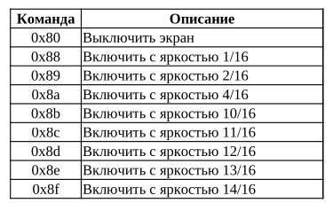
To adjust the brightness, use the following commands (a table translated and shortened by me from the documentation):
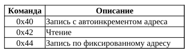
To select the transmission direction and addressing method, the following commands are available:
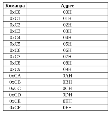
To transfer the address, commands starting with 0xC are used:
For those who are not in the know, just in case (just in case), I’ll explain that if a number starts with 0x or ends with h, then this means that it is written in the hexadecimal number system.
Everything seems to be relatively clear with the commands. The first difficulty I encountered was the strange memory addressing on the chip. After a little googling and reading the articles found, it became clear that the addresses of the indicators alternate with the addresses of buttons and LEDs.
A slightly modified sign from the documentation:
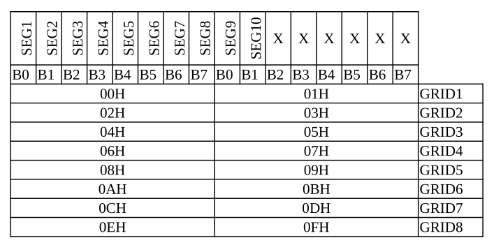
From it it is clear (or, in fact, not very clear) that even addresses from 00h to 0Eh are responsible for connecting seven-segment indicators. Odd addresses are for connecting buttons and LEDs. Moreover, the LEDs are connected to SEG10, and the buttons to SEG9.
Those. to display a number on the first indicator on the left, you need to write the data to address 00h. In order to light the first LED on the right, you need to write the number 2 at address 0fh (to turn it off, you need to write a zero).
Actually about the numbers. The documentation contains the pinout of the indicator and a diagram of its connection to the chip itself.
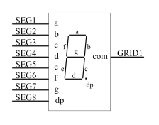
Those. segment a is the least significant bit, and dp is the most significant bit. In order to display the number zero, you need to light all segments except g and dp – this is 0x3f. To output one, you need to light segments b and c – this is 0x06, etc. The table shows binary and hexadecimal codes for all digits.
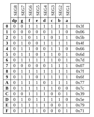
In my table with numbers, the bits are located least significant on the right; in the table of addresses from the documentation, the least significant bit is on the left. I’m more accustomed to placing the least significant bits on the right, so I drew myself a table with numbers this way; if it’s so difficult for you to perceive, you can mirror it. Although in the program, most likely, you will still write the least significant bit on the left, at least that’s how it works for me.
After reading the documentation on the diagonal, and a couple more articles on the Internet, I began to connect the TM1638 module to the Arduino Nano. To do this, I needed to look into the aruina pinout and select the hardware SPI pins there. The results were: pin 13 – SCK, pin 11 – MOSI, pin 10 – SS (three legs, since we have half-duplex).
Having connected the library, I wrote code for transferring data to the board and it didn’t work – it got stuck on the very first library function, the initialization function. Scratching my head, I decided that I didn’t want to delve into a library I didn’t understand and decided to do it without it (especially since reception through it still couldn’t be implemented due to the half-duplex connection). True, to make my work easier, I used the built-in shiftOut function, but, thank God, it worked, although I was already mentally ready to write it.
I chose different legs, but in fact it doesn’t matter at all. My command transmission looked like this:
void transfer (uint8_t data){
 digitalWrite (SS,LOW);
 shiftOut (DATA_PIN, CLK, LSBFIRST, data);
 digitalWrite (SS,HIGH);
 _delay_ms(100);
}
Where SS is the pin to which the STB input of the TM1638 module is connected, CLK is the SCLK input of the module, DATA_PIN is the DIO input. For me these were pins 10, 12 and 11 (PB2, PB4 and PB3). I also didn’t write the digitalWrite function using registers, because in this situation I don’t need it. The shiftOut function shifts the data, i.e. outputs bits one at a time per DATA_PIN pin, accompanying the transmission with clock pulses on the CLK pin. The LSBFIRST parameter indicates that the transfer will be carried out with the most significant bit first (yes, the documentation indicates that the transfer should be carried out this way).
Having used this function to issue a command to turn on and adjust the brightness, a command to adjust the address increment (in this case, only an entry with a fixed address is suitable, since the addresses are not in order), the address itself and some data, I expected that everything will earn. The screen lit up (already progress) and brought out all the garbage.

Having spent a lot of time re-reading documentation and articles on the Internet, I could not solve this problem. Although I did everything according to the example, it turned out to be incomplete. Thanks to my colleague, he was able to Google what I was doing wrong. It turned out that after transmitting the cell address, there is no need to raise the chip selection wire (SS) and pause, but you need to transfer data immediately after the address.
In general, this is all described in the documentation and even with pictures, but I didn’t read all the way to it (as always).
Here, in fact, are the timing diagrams for data transfer from the documentation:
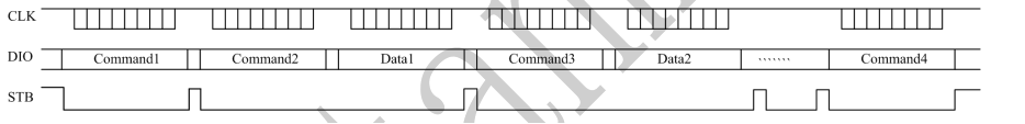
Where:
Command1: Set fixed address recording mode
Command2: set address
Data1: Send data to the address specified in Command2
Command3: set address
Data2: Send data to the address specified in Command3, etc.
Those. to send configuration commands, you must first lower STB to zero, send eight command bits (not forgetting to transmit pulses via CLK), raise STB (set logical one) and pause. In order to transmit data, you need to lower the STB, send eight address bits, then eight data bits, and only then raise the STB.
Based on this information, I added a second function for data transfer.
 void transferData(uint8_t addr, uint8_t data)
{
	digitalWrite(SS,LOW);
	shiftOut(DATA_PIN, CLK, LSBFIRST, addr);
  shiftOut(DATA_PIN, CLK, LSBFIRST, data);
  digitalWrite(SS,HIGH);
  _delay_ms(100);
}
In general, after all the ordeals, it started working and displayed beautiful numbers.

To perform button reception, I tried to use the shiftIn() function. And it didn't work. According to the documentation, when sending a read request, the board should return four bytes one after another, in which the bits corresponding to the pressed buttons are set to ones. I accept 32 zeros. I will continue my attempts and describe the result next time.
Full twenty line code Here.
I would be glad if this was useful to someone.