Will 2D semiconductors save Moore’s Law?
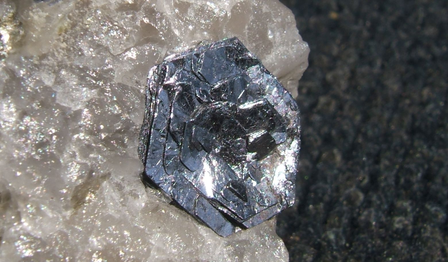
The use of molybdenum disulfide as a lubricant has been known since the 17th century, when settlers used it to lubricate carriage axles. Since the 1940s, the substance has been widely used as a component of lubricants. In nature, molybdenum disulfide occurs as a mineral – molybdenite (pictured)
Moore’s Law is an empirical assumption that the number of transistors in integrated circuits doubles every few years. However, this law began to malfunction, as transistors are now so small that current silicon-based technologies cannot offer further opportunities to reduce their physical size.
A group of scientists from the University of New South Wales (Australia) and the University of California at Los Angeles (UCLA) published a description of the technology for the production of two-dimensional semiconductors, which theoretically can solve the problem.
Two-dimensional semiconductors allow the propagation of electrons along the plane, which has a number of advantages: 1) very convenient switching of the transistor from open to closed state and vice versa; 2) directional motion of electrons without scattering, that is, on two-dimensional materials, you can make transistors with zero electrical resistance, which do not waste energy at all when turned on / off. Such materials are called superconductors.
If the resistance is zero, then what happens, superconducting processors will not heat up at all?
However, about everything in order.
Yes, in theory we can actually get zero resistance transistors. But in fact, there are many technological barriers that need to be overcome to create such advanced ultra-thin semiconductors. One of the obstacles is that the deposited ultra-thin films are too heterogeneous, that is, with grain boundaries. These boundaries represent the interface of two crystallites in a polycrystalline material, a defect in the crystal structure. The charge carriers seem to bounce off them and, therefore, resistance losses increase.
One of the most promising ultra-thin semiconductors is molybdenum disulfide (MoS2), the electronic properties of which have been studied over the past two decades.
However, obtaining a two-dimensional MoS2 on an industrial scale proved to be a real problem. No industrial MoS deposition technology yet2 has not demonstrated the possibility of obtaining a film without grain boundaries, which is critically important for the semiconductor industry. And this is where we come to scientific workwhich was published by researchers at the University of New South Wales School of Chemical Engineering and UCLA. They developed a new approach to MoS self-precipitation2, which allows you to eliminate the grain boundaries mentioned above.
The unique ability to eliminate graininess is achieved by using gallium metal in a liquid state. Gallium is an amazing metal with a low melting point of only 29.8 ° C. This means that at room temperature it is solid, but if you take it in the palm of your hand, it immediately melts. It becomes liquid, so its surface is atomically smooth. In doing so, the liquid remains a metal, so that the surface provides a large number of free electrons to facilitate chemical reactions.
By bringing the sources of molybdenum and sulfur closer to the surface of liquid gallium, more precisely, a eutectic alloy of indium with gallium, scientists were able to implement chemical reactions that form molybdenum-sulfur bonds in order to obtain the necessary MoS film2… The formed two-dimensional material is deposited on an atomically smooth gallium surface, so it naturally forms a perfectly flat shape without graininess.
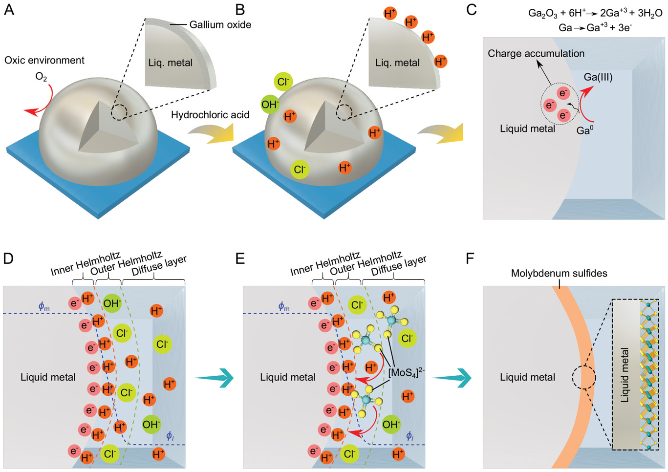
Self-precipitation MoSx on the surface of an indium-gallium eutectic alloy (EGaIn). At further steps of the technological process, a two-dimensional semiconductor film with an ideal structure without graininess is obtained. The process can be carried out on an industrial scale
The illustration above shows how MoS self-precipitates.2… The illustration below shows the sheets themselves.
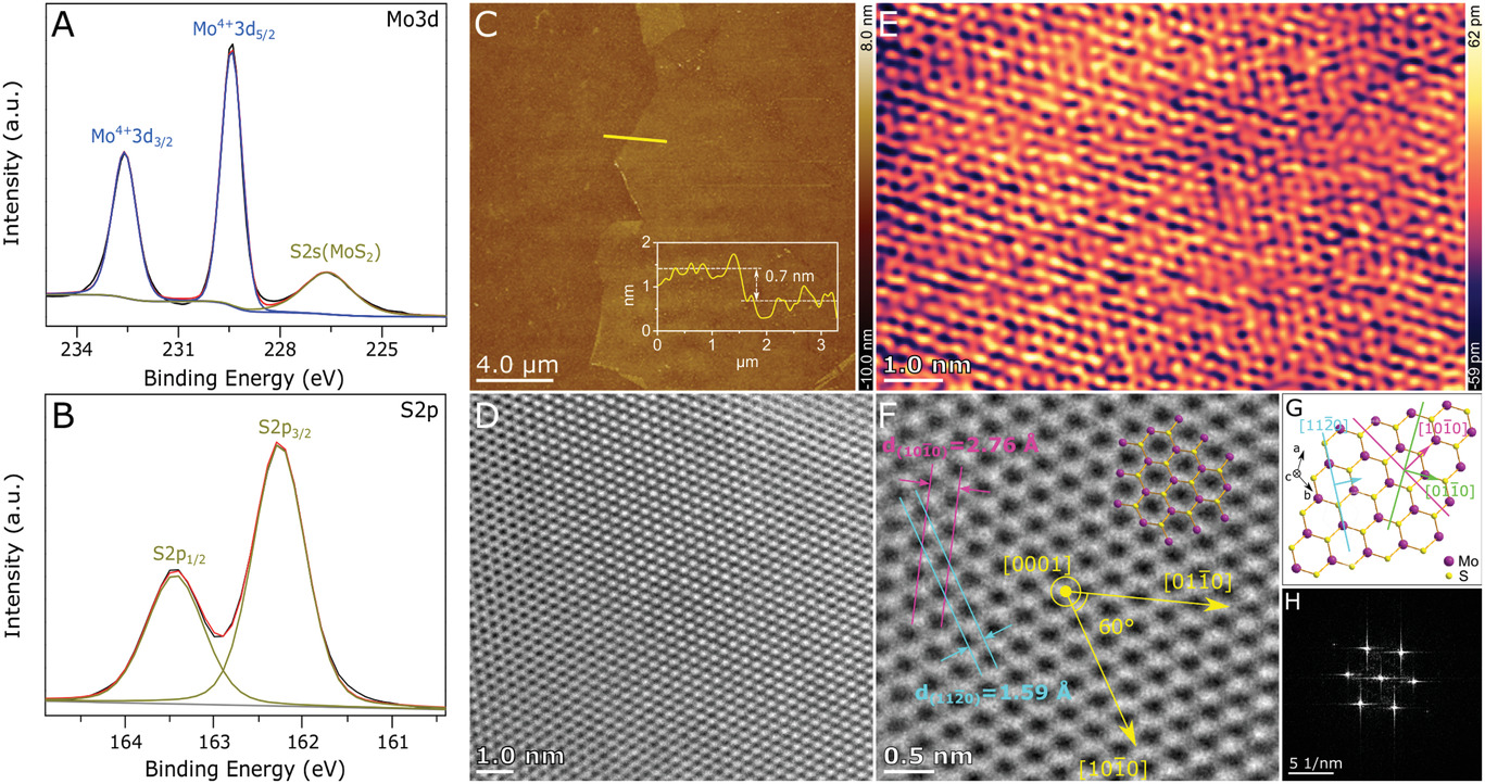
High Resolution X-ray Photoelectron Spectroscopy of MoS Crystalline Sheets2… Illustrated G and F: crystal diagram and real octagonal crystal structure
This is a very important step for the industrial production of super-smooth planar semiconductors.
UNSW researchers plan to improve the technology to create other two-dimensional semiconductors and dielectric materials that are used in microelectronics. The scientists emphasize that this method represents a versatile deposition procedure for any large two-dimensional transition metal dichalcogenide (2D TMD or TMD) that can be adapted for large-scale production, replacing traditional 2D TMD methods.
Scientific article published on October 2, 2020 in the journal Advanced Functional Materials (doi: 10.1002 / adfm.202005866).