Technology of electron-multi-beam lithography
Let’s start with the problem.
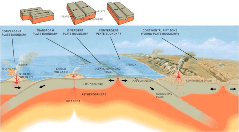
From every “iron” we hear about nanometers in microelectronics. Those who are a little deeper into the topic have heard that lithographs are used to obtain the coveted nanometers and that the most advanced chip manufacturers are switching from lithographs to DUV (Deep Ultra-Violet, Deep ultraviolet with a wavelength of 193 nm) to EUV (Extreme Ultra- Violet, Extreme ultraviolet with a wavelength of 13.5 nm).
But in order to get a drawing on a plate, you must first get it on a photomask. Moreover, the drawing on the photomask is often much more complicated than the resulting imprint on a silicon wafer. This is done to suppress the effect of “proximity” and suppress the effects arising from diffraction.

Although the size of the photomask pattern is usually 4 times larger than the final pattern on the plate, however, the accuracy of its manufacture must be no worse than the accuracy of the pattern on the plate, because. all “torn” edges and “rounded” corners on the photomask will be enhanced on the plate by more than 4 times.
To a certain limit, or rather, for photomasks for a manufacturing process up to 180 nm, laser photomask generators are used. But for technical processes from 180 nm and less, using a laser beam, it is no longer possible to achieve the accuracy required for photomasks. And here the use of electron beam lithographs begins. Because the wavelength of an electron is several orders of magnitude smaller than the length of ultraviolet radiation, then it becomes possible to draw structures with an accuracy of 1-5 nm with a beam of electrons.
But … as always there is this “but” …
The exposure rate of an electron-beam lithograph is orders of magnitude lower than the exposure rate of a laser photomask generator.
It may take up to several days for one photomask, and given that a complete set of photomasks for a microcircuit can consist of 80 pieces. these photomasks, the production time for a set of photomasks (masks) may take several months.
Considering the cost of an electron beam lithograph (about 15 million USD), it becomes clear why a set of masks for the 130 nm process technology can cost 500 thousand USD, and for an advanced 7-14 nm process technology can easily cost 10 million USD.
Maybe you should speed up?
Yes, it’s worth it. Therefore, the idea was naturally born to repeat the principle of operation of laser image generators, which use up to a million simultaneously controlled laser beams for illumination. These beams are reflected from micro-mirrors, which programmatically “twitch” and throw the laser beam either onto the plate (through a special micro-hole), or past (to the absorber). This is how an image is formed on the illuminated plate.
It looks beautiful – hundreds of thousands, or even a million electron beams, simultaneously irradiate the plate with an incredible accuracy of 1-5 nm. We are getting a technology that makes it possible to completely abandon such an expensive link as photomasks. And it is possible to produce prototypes, small and medium batches of chips at reasonable prices!
But … Again, this “but” … “It was smooth on paper.”
From here we will begin the description of the available options for electron-multi-beam technologies and the problems on the way to their implementation.
The technology from IMS Nanofabrication (IMS-NANO) is the most “simple”.
The most modest participant in the electronic technology competitiona lot of-beam lithography, but achieved tangible commercial results.
Within the European program MAGIC (MAskless lithoGraphy for IC manufacturing), 11.75 million euros were allocated to support MAPPER and IMS Nanofabrication.
IMS Nanofabrication AG (Austria) initially developed the project of ion-a lot of-beam lithograph CHARPAN (Charged Paarticle Nanotech).
By February 2009, a proof-of-concept sample was created. On hydrogen ions with an energy of 10 keV with a beam diameter of 12.5 nm, a resolution of less than 16 nm was obtained on the HSQ resist. The number of rays in the matrix is ~43’000 pcs.
But hydrogen ions are an undesirable element that remains in the silicon substrate after the photoresist is illuminated.
Therefore, starting from 2009, the company shifted its attention to the development of electronica lot of-beam lithograph under the RIMANA project (Radical Iinnovation Maskless Nanolithography), also with financial support from the European Commission. Moreover, at first, the aperture and quenching matrix from the project of ion-multi-beam lithography were used.
, RIMANA project (right)")
The electron-beam column designed by RIMANA allowed using only 2’500 beams out of a possible 43’000. Therefore, from the fourth quarter of 2009, work began on the creation of a new column and matrix for it.
By 2013, an electron-beam lithograph was assembled with a matrix of 262’144 (512×512) beams with a spot diameter of each beam of 20 nm.
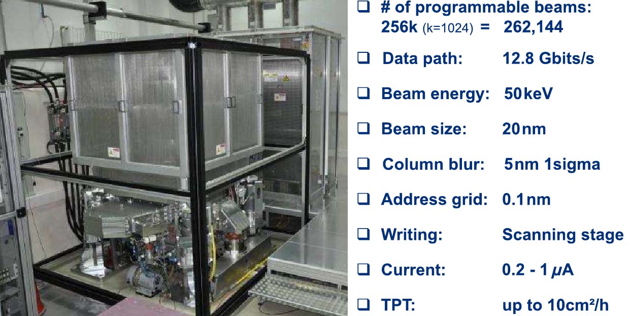
Setting the proof-of-concept level IMS-NANO – eMET Photomask Exposure Machine (eelectronic Mask Exposure Tool):
|
Number of programmable beams (# of programmable beams) |
262’144 pcs. |
|
data flow |
12.8 Gbps |
|
electron energy (Beam energy) |
50 keV |
|
beam size |
20 nm |
|
blur (Column blur) |
5nm 1sigma |
|
beam positioning grid (Address grid |
0.1 nm |
|
writing method |
table scan |
|
total column current (Current) |
0.2-1 uA |
|
performance (TPT) |
up to 10 cm2/hour |
The company decided to increase the spot size to 20 nm – this allows to increase performance by increasing the spot current, and by partially shifting the spot to an incomplete spot size and controlling the exposure time, it is possible to create topology elements with sizes of 1/3-1/2 of the spot size.

So, when the spot is shifted by half its size and the exposure time is 33% of the total, it is possible to obtain a topology element with a size of 10 nm. Lithograph from IMS allows you to control the displacement of the spot with an accuracy of 0.1 nm
IMS Nanofabrication decided not to miss the stars from heaven – to build a device capable of competing with projection lithography devices from ASML (a monopolist in the lithography market for microelectronics). The company took a firm path – the construction of an electron beam column according to the classical scheme worked out on electron beam microscopes. WITH Notcritical current of the electron gun and with Nothigh currents in individual beams.
The rejection of limiting currents made it possible to use the generally accepted electron-optical circuit with crossovers (in places where individual beams intersect), and, accordingly, to use well-studied macro-lenses and macro-deflectors for controlling and scaling the entire beam of rays at once. This greatly simplified the electron-optical circuit and circuit solutions of the control system.

The flow of electrons from an electronic source (Electron source) is collimated by electrostatic condenser multielectrode optics (Electrostatic multielectrode condenser optic). A programmable aperture plate (APS), consisting of an aperture plate (Aperture plate) and a blanking plate (Blanking plate), forms a beam of rays. Electrostatic multielectrode accelerating lens (Electrostatic multielectrode accelerating lens) increases the energy of electrons to 50 keV and focuses in the 1st crossover.
The 1st magnetic lens focuses the beam into the 2nd crossover at the center of the Stopping plate at 2nd cross-over. The electron beam that was slightly deflected by the blanking plate (bright green) does not enter the 2nd crossover, but is absorbed by the stop plate. With the help of a multipole deflecting (difflector) system (Beam steering multipole), the electron beam can be deflected, thereby illuminating the gaps between the beams and, if necessary, compensating for the movement of the continuously moving scanned table (Scanning stage). The 2nd magnetic lens finally focuses the beam onto a Resist coated 6” mask blank.
The total scaling (reduction) created by the electronic optics is 200x (Electron beam projection optics with 200x reduction).
. The photo shows a plate from the CHARPAN project assembled, consisting of aperture and blocking plates")
Although the technology does not have outstanding performance indicators (10 sq. cm per hour), relative to other technologies, electronica lot of-beam lithography, but is an order of magnitude superior to the performance of electronicone-beam lithography.
And relative simplicity, allowed to bring it to a commercial industrial level for the production of photomasks. Currently, the company is expanding its presence in the markets of Taiwan, South Korea and the United States.
First exposure results:
 30 nm +45 deg. -45 gr. positive HSQ resist (left), negative pCAR resist (right), electron beam 20 nm, electron energy 50 keV, b) Horizontal and vertical periodic lines with half pitch 24 nm (HP, half pitch), electron energy 50 keV, electron beam cross section 20 nm, aperture 4 µm,")
 Isolated 24 nm lines at various angles on a positive HSQ and a negative pCAR resist (labeled with 30 nm lines), electron energy 50 keV, electron beam 20 nm, aperture 4 µm, scaling 200:1.")
 of exposure obtained on a maskless electron multibeam lithography system. HSQ resist, 50 nm layer, 15 keV electron energy, 17.5 nm electron beam, 3.5 µm aperture, 200:1 zoom.")
The first results shown in the pictures are comparable to the best results for EUV lithography (wavelength 13.5 nm) from ASML, but the exposure speed does not compete with projection lithography technology for mass production of microcircuits. The market for technology from IMS Nanofabrication remains the market for photomasks (by the way, it reached 4.2 billion USD in 2021), the market for prototypes and small batches of microcircuits.
More about Mapper and KLA-Tencor technologies in the following articles.