Optical Chips in a Petri Dish and Quantum Networks – Master’s Degree in ITMO Megafaculty of Photonics
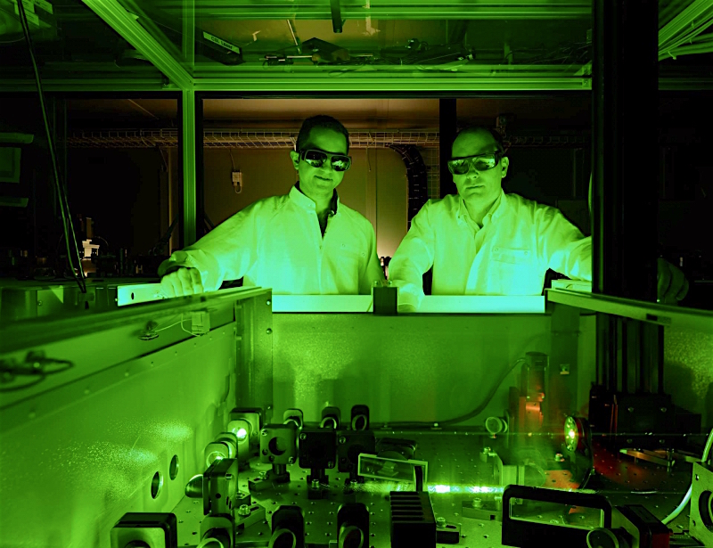
Photo ITMO University
A few words about the mega faculty of photonics
It unites four faculties: applied optics, laser photonics and optoelectronics, photonics and optoinformatics, and physical and technical. Here they study technologies related to the processing of light radiation and optical signals.
“If information technology is the industry of the present, then photonics is the industry of the future. The global photonics market currently amounts to $ 550 billion, but by 2023 it will reach approximately $ 800 billion, which ensures an increase in the demand for qualified specialists, including in Russia. ”
– Vladislav Bugrov, director of the mega faculty of photonics
In the photo: Vladislav Bugrov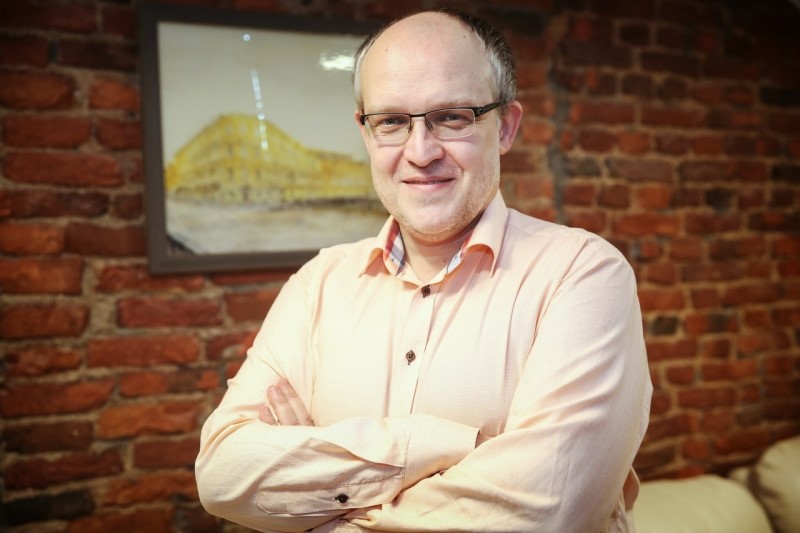 Employees, undergraduates and graduate students synthesize materials with non-existent optical and electromagnetic properties in nature, develop quantum technologies. For example, in 2017 at the megafaculty launched the first quantum network in Russia and the CIS. This is a data transmission system in which information is transmitted using photons and is reliably protected from wiretapping and hacker attacks.
In the future, banks will use the technology. They will receive even more secure communication channels between departments and units. The use of quantum networks will also find intelligence and telecommunications companies.
In early summer, a group of engineers under the guidance of specialists from the New Physics Institute of ITMO suggested the method of “growing” optical chips in an ordinary Petri dish. For the waveguide, the specialists chose gallium phosphide, and for the microlaser, the halide perovskite. The materials are placed in a cup with a solution of perovskite ink, and a light source grows on the waveguide. After that, the laser with the waveguide is left on the substrate and form the basis for the optical chip. The emission range of such a system exceeds the capabilities of analogues with silver or silicon nanowave guides. The size of the chip elements is three times smaller.
“On the Faculty of Physics and Technology ITMO conducts fundamental and applied research in the field of nanophotonics, radiophysics, solid state physics, as well as interdisciplinary research at the intersection of physics, chemistry, computer science, biology. They include metamaterials, optoelectronics, targeted drug delivery, topological photonics, biophotonics, optomechanics, wireless energy transfer, radio physics and other areas. The faculty has six international laboratories equipped with modern research equipment, which employs a large team of young scientists. ”
– Julia Tolstoy, engineer of the Faculty of Physics and Technology
Students also engage in scientific work – it often results in publications in thematic journals (Nature Communications, Journal of Physics, Nanophotonics and others) and speeches at international conferences.
Let’s talk about the directions of scientific research of undergraduates of the megafaculty.
Nanophotonics and metamaterials
Here, new materials with unique optical properties and optical control methods are studied – the way light interacts with matter.
“Undergraduate and graduate students from the very first semesters of study fall into scientific practice in the laboratory and instantly grasp everything. Often, they are already much better versed in individual issues, and they already explain the details of the work – it’s wonderful ”
– George Zograf, graduate student of the Faculty of Physics and Technology ITMO
They conduct both theoretical and practical research – the results are recognized globally. In 2015, our students, together with teachers, were able to predict the existence of a new type of electromagnetic surface waves – hyperbolic plasmon polaritons. Later guesses were confirmed experimentally, and over the past five years, these electromagnetic states have been detected in the microwave, infrared and optical ranges.
Photo: Who’s Denilo? / Unsplash
In the future, they can become carriers of the optical signal and used in information processing and transmission systems.
“During my graduate studies, my colleagues and I theoretically predicted a new type of electromagnetic surface waves, which are now known in the world as hyperbolic plasmon polaritons. In 2015, based on the results of this work, we published an article in the authoritative journal Physical Review B, while the editors of the magazine highlighted and recommended our work ”
– Oleg Ermakov, graduate and curator of the program “Nanophotonics and Metamaterials”
In the photo: Oleg Ermakov ITMO University cooperates with a large number of partners – the international center of the Research Center of Nanophotonics and Metamaterials, research laboratories and universities.
Weekly open seminars are held at the faculty on topical issues in radiophysics, optics and theoretical physics with the participation of foreign and Russian scientists.
Students have the opportunity to go to international scientific internships with training in English and receive a double diploma from one of the European universities. Masters receive the skills necessary for working in large specialized companies specializing in optical technologies – these are Samsung, Bosch, Huawei and Corning.
Some students decide to launch their own projects – in this case, the faculty provides support. A number of graduates decide to continue to do science and continue their academic careers in educational institutions in Russia, China, America, Singapore, Australia and other countries.
“During my undergraduate studies and when I entered graduate school, I didn’t even think that I would be a scientist – I just loved physics. Before me again was an important choice – where exactly to go to graduate school. I received offers from several European universities, but still decided to pursue a career in ITMO. During my studies at ITMO graduate school, I also worked a lot and presented my results abroad. In particular, over the past two years I have had three internships at the Technical University of Denmark and two internships at the Leibniz Institute of Photonic Technologies in Germany. In addition, I attended a number of conferences and symposia not only in various cities of Russia, but also in France, Italy, Denmark and even Singapore. ”
– Oleg Ermakov
Semiconductor Physics
The educational program is based in partnership with the Physicotechnical Institute. A.F. Ioffe. Students in this direction study the theory of photonic structures, solid state optics, electrodynamics of metamaterials, physics of semiconductor nanostructures, as well as linear and nonlinear magnetophotonics and nanoplasmonics.
Graduate students can choose for themselves a specialization – courses in theoretical or experimental physics (although attending classes in both areas is not forbidden). The theoretical track involves an in-depth study of individual sections of quantum mechanics, as well as numerical methods in the physics of semiconductors. As for the experimental track, it includes a series of laboratory works to familiarize with the technology for the production of semiconductor structures.

Photo: Karsten Würth / Unsplash
Students and university professors have already implemented several projects in this area. In 2017, they have developed A new coating for solar panels based on amorphous silicon. Engineers changed the structure of the upper electrode of the solar cell – glass objects in the form of a droplet in the size of a micrometer were immersed in it. They focus light in a semiconductor layer and reduce the reflection of rays.
“This method allows you to form the structure of the electrode, literally aligning it with atoms. A very high-quality coating is formed that gives good conductivity. As a result, the overall efficiency of the solar panel increases by 20%. Such an electrode with glass inclusions can be used for thin solar cells based not only on amorphous silicon, but also on any other materials. ”
– Mikhail Omelyanovich, graduate student of the New Physics Institute ITMO
In addition to Nanophotonics and Metamaterials and Semiconductor Physics, we have two physics programs based on the photonics megafaculty – LED Technologies and Optoelectronics and Information Technologies in Thermophysics. We will tell you more about them next time.
About other directions of the magistracy:
- “Food, Economics and Resource Management”: Biotechnology in ITMO’s Master Program
- What they do at the faculty of low-temperature energy at ITMO University