NE555 integral timer and its application
When the production of the NE555 integrated timer chip began in 1972, no one imagined that in fifty years it would not lose popularity, and the word “legendary” would be added to the name of the timer.
In this publication, we will analyze the main applications of the legendary 555 timer and carefully look at it “under the hood”.
The circuits given as an example and the timing diagrams of the operation of these circuits were created using the TINA TI V9 SPICE simulator (version 9.3.150.328). The NE555 integral timer model is taken from the simulator’s standard library.
Important information: the parameters of the generator used in the examples with the Schmitt trigger and the waiting multivibrator were set through the properties of the generator and the “Signal Editor” called from there. The transient analyzer was launched with the “Zero Initial Conditions” option selected.
Using the 555 timer as an RS flip-flop
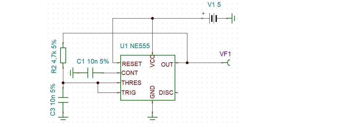
The simplest application of the 555 integral timer is to use it as an RS flip-flop. The “classic” RS flip-flop has two stable states, the transition between which is carried out by applying control signals to the reset and installation inputs. The scheme for switching on the 555 timer as an RS flip-flop is shown below:
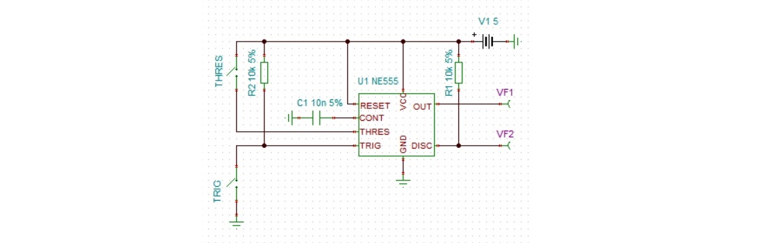
The “TRIG” input is used as the S (Set) input: when you press the “TRIG” button, the input of the microcircuit is connected to a common wire, and a high logic level is set at the output.
The “THRES” input is used as the input R (Reset, reset): when the “THRES” button is pressed, the supply voltage is applied to the input of the microcircuit, and the output of the microcircuit goes into a reset state.
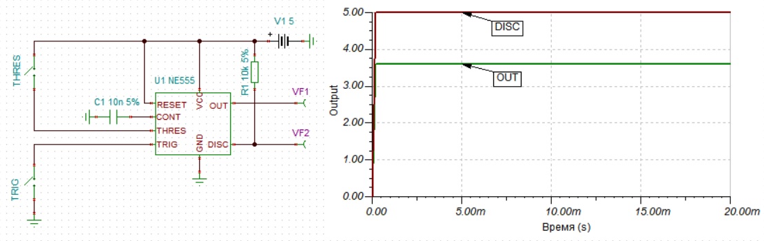
An important element of the circuit is the “pull-up” resistor R2. Without it, a high logic level is set at the output of the microcircuit immediately after switching on, and the device does not respond to button presses. Transients when the RS flip-flop is turned on without a “pull-up” resistor R2 are shown in the graph on the right:
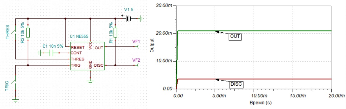
If there is a pull-up resistor at the TRIG input, the microcircuit output is set to a low logic level (reset state) when it is turned on, and the device changes state depending on the state of the inputs. The graph of transients when turning on an RS flip-flop with a “pull-up” resistor is shown below:
Block diagram of the 555 timer
To deal with the behavior of the microcircuit, which is not quite characteristic of the “classic” RS flip-flop, we will study its block diagram. Let’s take TI’s NE555 integral timer as an example. The block diagram looks quite curious:
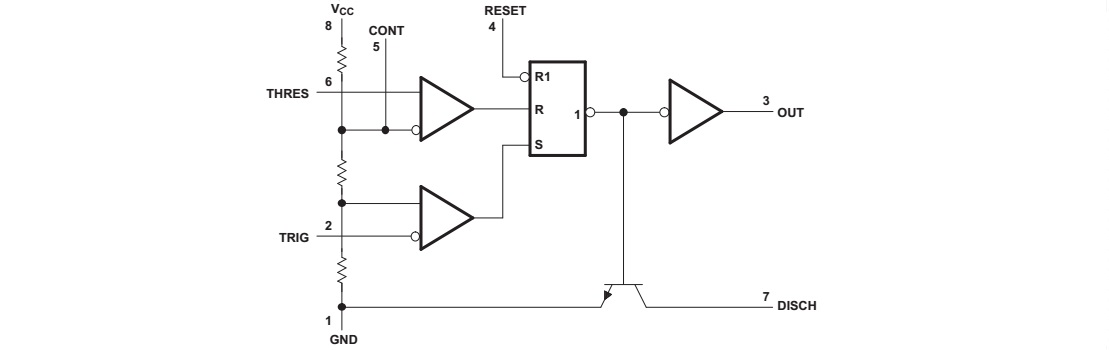
In the center of the composition is an asynchronous RS flip-flop, the inverting output of which is connected to an inverting output buffer and an open-collector transistor switch. The trigger is reset either by a low logic level signal at input 4 “RESET”, or by a high logic level signal at the output of the top comparator according to the circuit. The trigger is set by a high logic level signal at the output of the lower comparator according to the circuit.
The thresholds for the comparators are set by a voltage divider of three resistors. The voltage of the upper threshold is applied to pin 5 “CONT”.
The RS-flip-flop is set when a voltage is applied to input 2 “TRIG” below the lower threshold, provided that a high level voltage is present at the “RESET” input.
The reset of the RS-trigger occurs when a voltage is applied to input 6 “THRES” above the upper threshold, provided that a high level voltage is present at the “RESET” input, and the voltage at the “TRIG” input is above the lower threshold.
Thus, the RESET input has the highest priority, and the TRIG input has a higher priority than the THRES input. When the NE555 is turned on according to the RS-trigger circuit without “pull-up” at the “TRIG” input, the voltage below the lower threshold will always be present at the “TRIG” input, and the output will go into the reset state only for the time the low-level signal is applied to the “RESET” input .
I just want to emphasize and draw attention: in most sources, the comparator thresholds are indicated as 2/3 Ucc and 1/3 Uccand the “CONT” pin is used as an output shunted by a 0.01 uF capacitor, or not connected anywhere, but with pin 5 “CONT” it’s not so simple.
The datasheet from TI “xx555 Precision Timers. SLFS022I – September 1973 – Revised September 2014” pin 5 is labeled I/O and the thresholds are labeled “CONT” and “1/2 CONT”. This means that the levels of the comparator thresholds are not “fixed” to the timer supply voltage, but can vary over a wide range by applying a control voltage to the “CONT” input. If the control voltage is not applied to pin 5, it is used as the “CONT” output with a 0.01 uF shunt capacitor connected to it, and the upper threshold in this case is CONT = 2/3 Ucc.
The use of a shunt capacitor increases the stability of the microcircuit and its noise immunity. Also, do not forget about connecting blocking capacitors to the power circuits of the microcircuit.
The supply voltage range of most models of the 555 series timers is from 4.5 to 16 V (up to 18 V for some models), the current consumption varies from fractions to units of a milliamp (depending on the model), the output stage of most models is capable of withstanding current up to 200 mA.
Using the 555 Timer as a Schmitt Trigger
The Schmitt trigger is used to convert a non-rectangular input signal to a rectangular output signal. A characteristic feature of the Schmitt trigger is the presence of hysteresis, which is determined by the width of the “window” between the levels of the trigger.
Using the 555 timer as a Schmitt trigger is another use for this IC. To do this, you need to apply an input signal to the timer’s TRIG and THRES inputs connected together. The amplitude and offset of the input signal must be such that the signal overlaps the “window” formed by the thresholds of the comparators.
In the figure below, a triangular signal with an amplitude of 2 V and a bias U is applied to the input of the Schmitt trigger.offset = 2.5 V, equal to half the supply voltage Ucc. Signal frequency 1000 Hz. In this case, the upper threshold of the comparator Ucont = 2/3 Ucc = 3.33 V, and the lower threshold of the comparator 1/2 Ucont = 1/3Ucc = 1.67 V.
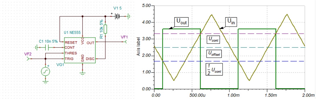
On the graph, we see the conversion of the input periodic signal of a triangular shape into a classical square wave with DC = 50%, where DC is an abbreviation for “duty cycle” (duty cycle). The input signal can be of any shape, “triangle” as the input signal was chosen for reasons of clarity.
Let’s try to use pin 5 “CONT” as an input and apply a voltage of 4 V from an external source to it. The output signal changes are shown in the figure below:
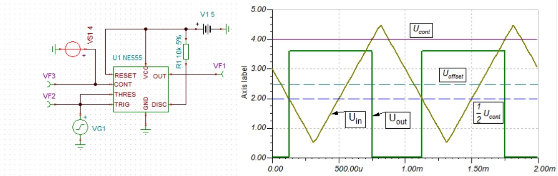
We see that for the same period of the output signal, its duty cycle has increased. This is due to the fact that the “window” of the comparator has moved up and expanded.
Now we apply a voltage of 2 V to the “CONT” input:
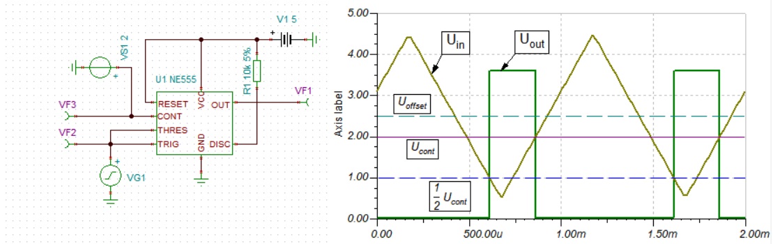
The fill factor decreased due to the fact that the “window” moved down and narrowed.
The above examples illustrate the possibility of pulse-width modulation (PWM) of the input periodic signal by the voltage at the “CONT” input.
The use of pin 5 “CONT” as an input also makes it possible to narrow the “window” of the comparator for converting signals with a small amplitude value. It is important that the input signal at the same time have an offset at which it would remain within the timer supply voltage.
Using the 555 Timer as a Multivibrator
A multivibrator is a relaxation oscillator with a rectangular output signal. It is relaxing due to the fact that the elements of the multivibrator do not have resonant properties.
The multivibrator circuit on the 555 timer and the diagram of its operation are shown in the figure below:
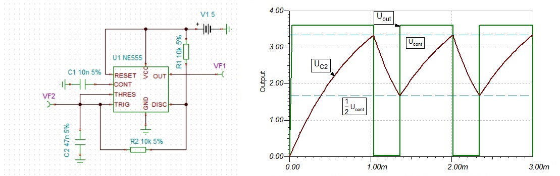
At the moment of switching on, a high logic level is set at the output of the microcircuit, the transistor switch closes, the resistance of the “DISC” output is high. Capacitor C2 is charged through resistors R1 and R2 connected in series to a voltage U
cont
, the output of the microcircuit is set to a low logic level, the transistor switch opens and connects the connection point of the resistors R1 and R2 to a common wire. Capacitor C2 is discharged through resistor R2 until the voltage across it reaches 1/2 U
cont
the output of the timer will not be set to a high logic level, the transistor switch will not close, and the capacitor will not start charging again through resistors R1 and R2 connected in series.
In auto-generation mode, the duration of the high level of the output signal of the multivibrator on the 555 timer is:
In this case, the duration of the low signal level:
and the period is:
It can be seen from the formulas that the temporal characteristics of the multivibrator on the 555 timer are determined by the values of the elements R1, R2, C2 and do not depend on the supply voltage of the microcircuit.
Apply a voltage of 4 V from an external source to the “CONT” input:
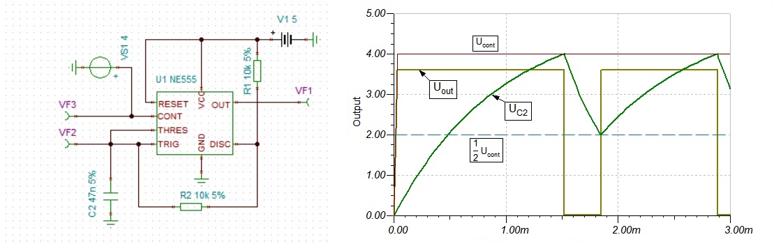
The period of the output signal and its duty cycle have increased.
When a voltage of 2 V is applied to the “CONT” input, the period of the output signal and its duty cycle decrease:
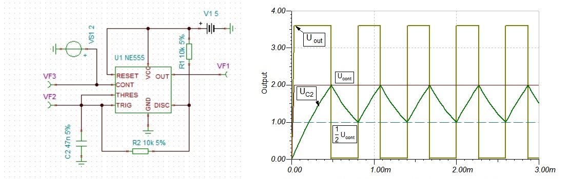
It can be concluded that a change in the voltage at the “CONT” input leads to pulse frequency modulation (PFM) of the output signal of the multivibrator.
Using the 555 timer as a standby multivibrator
The waiting multivibrator (single vibrator) is designed to generate a pulse of a certain duration according to an external event.
Usually, as an external event, the shorting of the TRIG input to the common wire by pressing a button is used, but instead of a button in the emulator, we will use a signal generator set to a single low-level pulse with a duration of 10 ms:
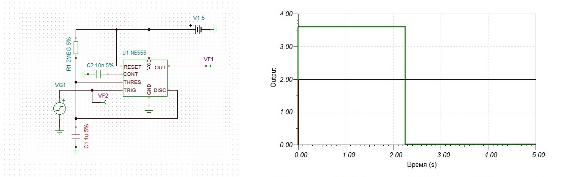
As can be seen from the timing diagram of the operation of the standby multivibrator on the 555 timer, upon receipt of a pulse, the circuit generates a signal at the output with a duration of about 2.2 seconds. The signal duration is determined by the formula:
I would like to draw attention to the fact that the duration of the output signal of the waiting multivibrator on the 555 timer also does not depend on the supply voltage.
▍ From the author
The publication provides a brief overview of the 555 integral timer and its main applications. Most of the devices cited in the publication can be implemented on microcontrollers, but NE555 analogues are still produced by the industry due to low cost and reliability.
An important feature of the circuits on the 555 timer is that the timing characteristics of these circuits do not depend on the supply voltage, and these characteristics are calculated using simple formulas or diagrams.
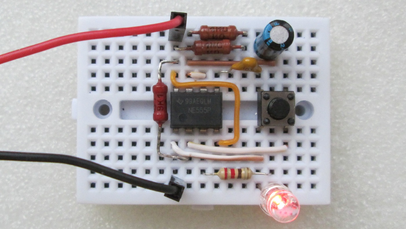
The 555 timer enjoys well-deserved popularity among beginner radio amateurs: it is inexpensive, the DIP-8 package is easily installed in a solderless board, and a minimum of “strapping” is required. And what is very important for the motivation of beginners: the circuits on the 555 timer start working immediately after the correct assembly.
Here is an example of the simplest generator on the NE555:
And according to the scheme from the section about the waiting multivibrator, a 12-year-old teenager assembles such a time relay in half an hour:
…and it all started fifty years ago, and I hope it won’t end soon.