How do processors actually do? Parsing
Here’s a seed for you – a 30-kilowatt laser in a vacuum shoots at a drop of tin and turns it into plasma – fantastic say?
And we will figure out how it works and tell you about one company from Europe, which stands as a shadow behind all the giants Apple, AMD, Intel, Qualcomm, Samsung and others, and without it there would be no new processors. And no, it is, unfortunately, not the Cheboksary Electronics Plant.
To understand the process of extreme ultraviolet lithography, we first need to understand what photolithography is. The process itself is very similar to how photographs are printed from film negatives onto photographic paper! Do not believe me – now we will explain everything.
Photolithography
Let’s start with a simple example – take a transparent glass and apply some kind of geometric pattern to it, while leaving some areas without paint. Basically, let’s make a stencil. Attach this piece of glass to the flashlight and turn it on. We will get exactly the same shadow pattern that we applied to the piece of glass.
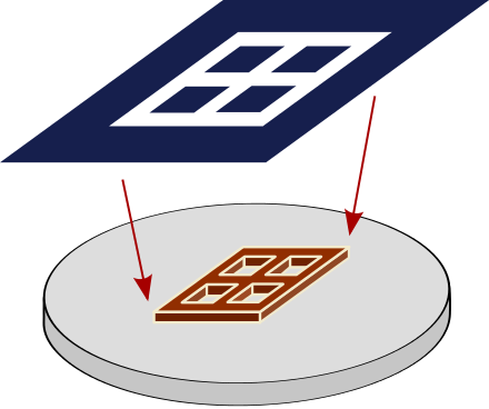
In the manufacture of processors, this piece of glass with a pattern is called a mask. The mask allows you to obtain on the surface of any material “overexposed and underexposed” areas of any flat shape.
Ok – we got a drawing on the surface, but it’s just a shadow. Now we need to somehow save it there. For this, a special light-sensitive layer is applied to the surface of the silicon wafer, which is called a Photoresist. For simplicity, we will not talk here about positive and negative photoresists, why they react this way, after all, we are not in a physical chemistry lesson. Let’s just say that this is a substance that changes its properties when light hits it at a certain frequency, that is, at a certain wavelength. 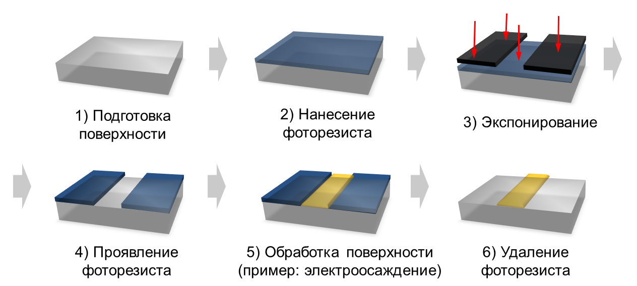
Again, just like on photographic film or photographic paper – special layers of materials react to light!
After we have illuminated the areas on silicon that we need, we can remove them, while leaving the rest, that is, non-illuminated areas, in place. As a result, we got the drawing that we wanted. This is photolithography!
Of course, in addition to photolithography, other processes are involved in the production of processors, such as etching and deposition, in fact, by combining these processes together with photolithography, transistors are, as it were, printed layer by layer on silicon.
The technology is not new, almost all processors since the 1960s are produced using photolithography. It was this technology that opened the world of field-effect transistors and the path to all modern microelectronics.
But the really big leap forward in this area only happened recently! With the transition to EUV. And all because of the long wavelength of 13.5 nm. Don’t worry, I’ll explain now!

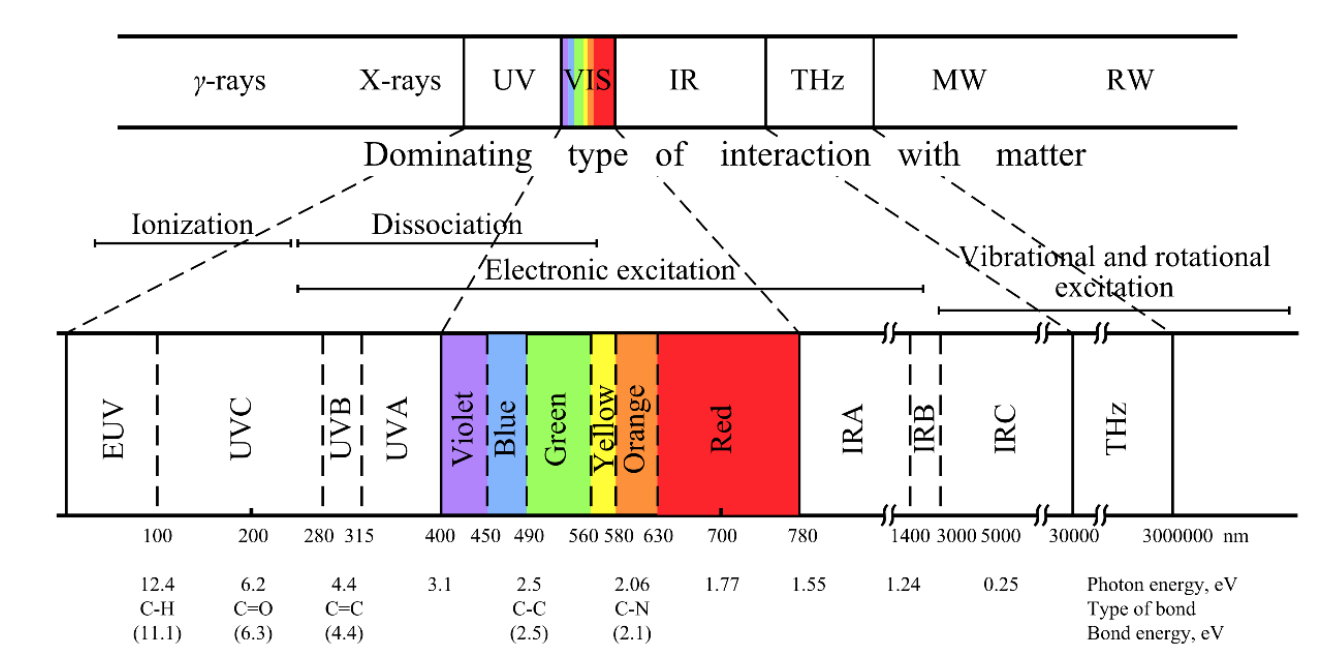
The wavelength at which our “flashlight” shines is an incredibly important parameter. It is she who determines how small you can get the elements on the crystal.
The rule is as simple as possible: Less wavelength means more resolution, and less process technology!
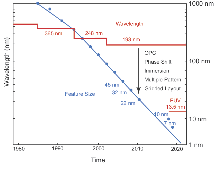
Pay attention to the picture. Absolutely all processors from the early 90s to 2019 were produced using the Deep UV lithography process, or DUV lithography. This is what it was before Extreme.
It was based on the use of an argon-fluoride laser that emits light with a wavelength of 193 nanometers. This light lies in the region of deep ultraviolet radiation – hence the name.
It passes through the lens system, the mask and onto our photoresist-coated crystal, creating the desired pattern.
But this technology also had its limitations, tied to the fundamental laws of physics.
What is the minimum technical process possible? We look at the formula (just don’t be alarmed):
![]()
Here Lambda is our wavelength, and CD is critical dimension, that is, the minimum size of the resulting structure. That is, using the “old” DUV lithography, it is impossible to obtain structures not less than about 50 nm. But how can you ask this? After all, manufacturers perfectly did both 14 and 10 nm, and some even 7 nm using DUV lithography.
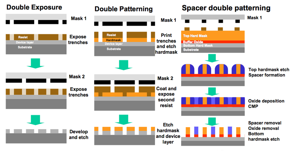
They went for tricks. Instead of a single glare through one single mask, they began to use several masks, with different patterns that complement each other. This process was named multiple exposure… Let’s call this the Puff Pie Principle!
Yes – the manufacturers bypassed direct physical limitations, but the physics did not deceive!
A serious problem has appeared: these additional steps have made the production of each chip much more expensive, because of them, the number of rejects increases, and there are other problems.
That is, in theory, you can continue to work with the old technology and by playing with masks and exposure (double, triple, quadruple exposure), reduce the size further, but this will make the process gold. Indeed, with each layer, the percentage of rejects grows higher and higher, and the error accumulates!
That is, we can say that DUV is a dead end! What to do next, how to reduce?
And here comes the great and terrible technology of Extreme UV lithography, or EUV lithography!
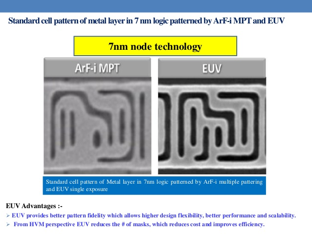
Look at the photo – it perfectly demonstrates the difference between the two technologies. Both were obtained using a 7-nanometer process technology, but the one on the left was obtained using DUV lithography and with the very tricks we talked about – triple exposure, that is, with the phased use of 3 different masks. On the right is the EUV lithography technology at 13.5 nanometers, using a single mask – the difference is obvious – the boundaries are much clearer, better geometry control, well, the process itself is much faster, the percentage of rejects is less, that is, in the end it is cheaper. Here it is the road to a bright future, why not do it right away, what is the problem?
How EUV lithography works
The thing is that even though EUV is the same lithograph, inside the details everything is much more complicated and here scientists and engineers faced new problems!
The technology of extreme UV lithography itself began to be developed at the very beginning of the 2000s. It uses a source that emits light with a wavelength of 13.5 nanometers – that is, at the lower end of the UV spectrum, close to X-rays!
In theory, this method can be used to create structures of already critical dimensions – so small that a little more and the laws of ordinary physics will cease to operate on them. That is, after 5 nm we find ourselves in the quantum world!

But even this problem has been solved at the moment. There is a source – take it, and make yourself arbitrarily small processors.
It’s not that simple at all!
The problem with these short wavelengths is that they are absorbed by almost all materials, so conventional lenses that were previously no longer fit. What to do?
To control this light, it was decided to create special reflective mirrored lenses. And these lenses need to be smooth! Very smooth !!! Almost perfectly smooth!
Here’s an analogy – let’s stretch the lens to the size of, say, Germany, so its area should be so smooth that nothing should stick out more than 1 millimeter. This parameter is called the lens roughness and the one we need should be less than 0.5 nanometer. This is already close to the size of an ATOM! Who can shoe a flea?
Of course, Zeiss – only they can do it! Yes – the same Zeiss company, whose lenses are on my camera, were in Nokia or in the flagships of Sony Xperia.

One problem solved – there are lenses!
There is a second – this light is scattered even in plain air. Therefore, in order for the process to proceed normally, it must be carried out in a vacuum!
I generally keep quiet about dust and dirt particles – it is clear that they should not be there at all. Clean rooms in such a production are orders of magnitude cleaner than operating rooms in hospitals! People literally walk in spacesuits. Any, even the smallest particle of air skin dirt can spoil both the mask and the mirrors!
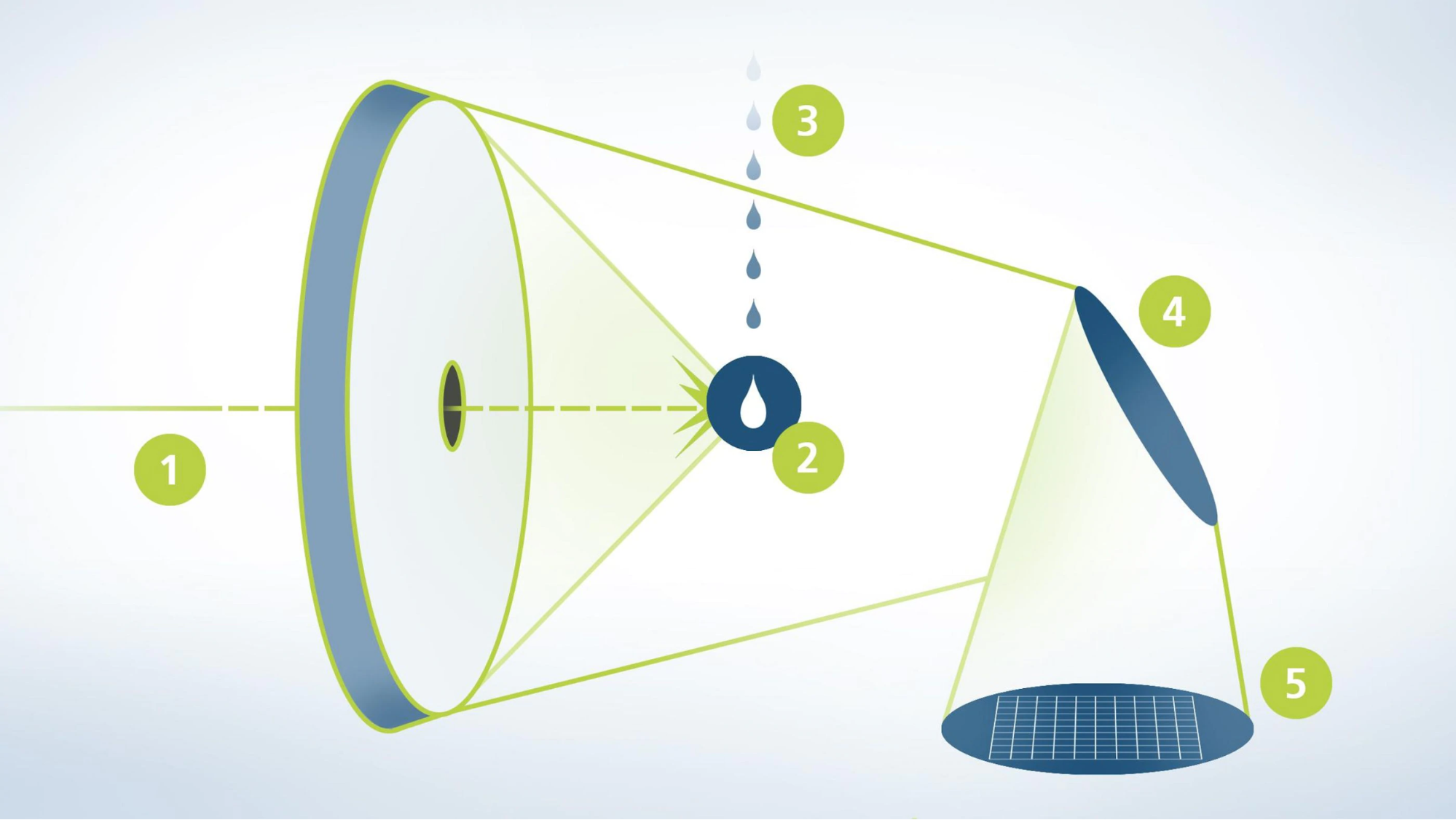
And what about the source? Just put a special laser at a shorter wavelength and that’s it? The problem is that neither bulbs, nor lasers, nor any other normal light sources that emit at this wavelength simply do not exist in nature.
And how, then, do you get the required radiation? Elementary, Watson – we need plasma.
It is necessary to heat the tin vapor to temperatures 100 times higher than the temperature of the sun’s surface! Just! And there are almost 2 decades of development behind this.
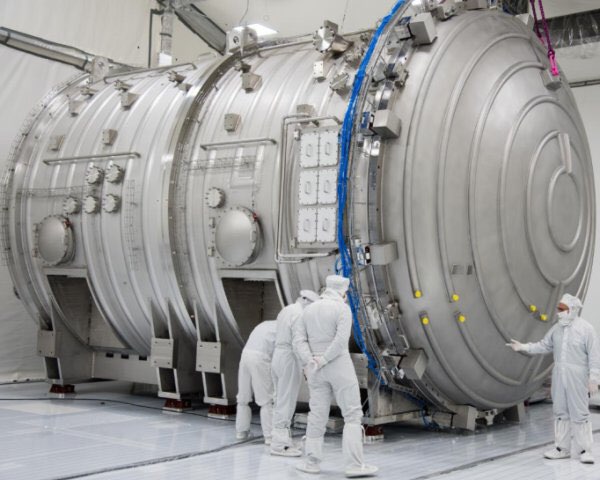
In the installation for the production of processors using EUV lithography, which we will talk about separately, a special carbon dioxide laser is installed, which, again, can be produced in tandem of only two companies in the world – the German company Trumpf and the American Cymer. This 30 kilowatt monster fires 2 pulses at a frequency of 50 kilohertz.
The laser hits the tin drops, the first shot actually flattens and turns the drop into a pancake, which becomes an easy target for the second volley, which sets it on fire. And this happens 50 thousand times a second! And the resulting plasma emits this light in the extreme UV spectrum.
And of course, this is only the very base, but we tried to paint you a picture of how difficult and cool this process is.
The company behind all processors
They talked about the technology, it means that someone invented and implemented it, but its development turned out to be so expensive that even large giants and bigwigs are not able to pull such budgets!
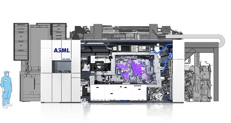
In the end, for this to become a reality, everyone had to chip in – Intel in 2012, and TSMC and Samsung took part in a common project somewhere in 2015. The total investment was, according to various estimates, from 14 to 21 billion dollars! Of which almost 10 billion were invested in a single Dutch company ASML. It is she who is behind all the production of processors in the world using the EUV lithography method! Wow! What is ASML and why haven’t we heard about it? A company from the Netherlands – what a dark horse?
The thing is that ASML has created the very tool without which Apple, Samsung and Intel with AMD are practically without hands! We are talking about an installation worth over $ 120 million. It is huge, 180 tons, consumes almost 1 megawatt of electricity, and needs almost 1.5 tons of water per minute to cool it down! But even with such a price, queues for them have been standing for years, because several dozen of these machines are produced a year.

It is also worth mentioning the considerable contribution of Russian minds. For example, one of the creators of this technology is Vadim Evgenievich Banin, now the development director at ASML. Our other compatriots also work in the company!
We found out that this company makes one of the most technologically advanced devices, in which all the knowledge of mankind is collected and all IT giants produce processors on them at once!
But not only ASML is behind the backs of the well-known IT giants. Their installations consist of more than 100 thousand parts, which are manufactured by more than a thousand companies around the world. All these companies are related to each other!
Future
But what will happen next! Did you think that we will leave you in the day today? No – we peeped into the future! We got information about what will happen after five or even two nm!
Firstly, right now, while you are watching this video, TSMC is already churning out new processors for HUAWEI, Apple and Samsung using EUV lithography, but not at 7nm, as was the case with Apple A13 and Kirin 990, but on 5nm process technology! And there are many proofs of this! And we will hear about them this fall. How do you like that – the A14 Bionic will be 5nm! We are also waiting for the new 5nm Exynos and Google processors, which we talked about separately! Qualcomm will probably follow them too, but here we have no data!
And secondly, and this generally explodes the brain, ASML is already completing the development of installations that will make it possible to produce processors on a 2 nanometer process technology, and even less in just 4-5 years!
For this, the guys from the Dutch company, together with the German Zeiss, have developed new mirror lenses with high aperture values. These are anamorphic optics – and much more, they will allow you to increase the resolution.
The process itself is essentially the same EUV, but with the High-NA EUV prefix. And the units themselves will take even larger sizes, look this is how they make optics for them!
This year is difficult for everyone, but at the same time – look at what steps technologies are beginning to develop, more and more. We are waiting for new processors with capacities that we never dreamed of.
In addition, completely new types of processors are being developed, such as NPUs, for neurocomputing.