Digging into Apple’s M1 chip

The Apple M1, the first chip designed by Apple engineers for their own line of computers, outperformed many competing microprocessors and nearly every component used in other Apple devices (especially in single-core performance tests and graphics benchmarks).
Apple was kind enough to post a photo of the die (another small detail that brought the company closer to AMD and Intel, as it is now a traditional strategy for announcing new processors), and they were quickly taken apart by super-geeks like Andrei Frumusanu of Anandtech.
We know from earliest announcements that the ARM-based M1 will be a solid entry in the SoC category.
It will probably be easier for analysts to analyze processors assembled from chiplets (it is expected that such a CPU architecture will take out the traditional one). Because each chiplet is essentially a separate piece of silicon. To understand the architecture of the SoC takes a little (maybe a lot) of looking.
Selection of individual blocks (on the initially unallocated map) Apple M1
All of these efforts will benefit competitors and those interested in organizing silicon devices efficiently. As you know, the most popular advantage of a packaged system architecture that uses chiplets over monolithic devices is that SoC solutions quickly become complex, confusing, and expensive. This leads to the fact that not all companies involved in microcircuits can enter the SoC market. Understanding the design of best-in-class products and researching cutting-edge technology is more important than packaging chip design experience.
M1 features
The M1 has a number of distinctive features.
Firstly, very little space is allocated for the on-chip cache memory. Apple engineers focused on functionality, not memory. The UMA architecture used in the M1 frees up space on the die while providing fast access to LPDDR4X memory. UMA allows individual memory components to be shared both between the CPU cores and the GPU in order to optimize the chip structure. Maintaining the physical proximity of memory modules is a concept borrowed from mobile processors, in which memory is placed on top of the processors as in a packaged system architecture. This has been talked about a lot earlier – in short, a similar approach is used in computers to improve performance and efficiently dissipate heat, and the architecture taken from mobile devices ensures compactness and energy efficiency.
A significant part of the M1 chip is dedicated to the graphics module. You can tell yourself that this is not surprising. And so it is. Nobody expected Apple to sacrifice graphics performance. To some extent, this approach is also taken from the mobile architecture.
Another important aspect of the M1 chip design is that Apple has chosen to increase the number of logical cells (rather than physical cores). This is the advantage of developing processors for your own OS – some functions can be built into the firmware and offload the CPU to perform more complex tasks. A good friend of mine and a great technology analyst, Paul Boldt, has talked about this many times. One of his articles is a quote from Alan Kay, which I will insert into this text: “People who are really serious about software should make their own hardware.”
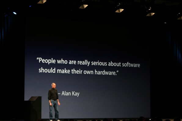
Steve Jobs quotes Alan Kay
An interesting opportunity is the flip-chip technology used to assemble the most advanced microcircuits. I wrote about it in one of my previous texts – it allows you to quickly obtain images with a chip device due to the transparency of silicon for infrared radiation. This approach saves time and money.
The Mac Mini’s ease of access to the M1 also allowed the chip to be monitored during benchmark testing.
Using a thermal imager, you can track the active areas of the chip by their temperature. In the image below as an example, there is a bright yellow spot – this is a high-performance core that is active while the computer is running. Thanks to early access to benchmarks (such as Geekbench 5) created specifically for the M1 processor, thermal analysis has revealed the location of the Firestorm and Icestorm cores, GPU and neural processors and many other components.
Temperature analysis has been very helpful and has opened the door to other testing methods. However, other computing platforms (especially mobile ones) make analysis difficult. But if there is a desire, then there will be a solution. More importantly (and obviously in the semiconductor market), if you have a sufficient budget, you will succeed.

Snapshot of M1 from a thermal imager in single core mode (Source: MuAnalysis)
While much of the focus on the M1 has to do with its architecture (and should be), it’s not just the technical details that are interesting in the design and structure of the processor. M1 BGA substrates with two side-by-side LPDDR4X memory modules and fully encapsulated BGA DRAM packages are identical (or very similar) to the mobile A-series processors used in the iPad – A12X and A12Z.
Probably the best tool for gaining a general understanding of the complex structure of a device, while providing image detail, is X-ray computed tomography. System Plus Consulting published an overview of CT scan results and analyzed the integration of both surface and wafer-embedded silicon decoupling capacitors in the M1. This chip information is part of a standard cost analysis from System Plus Consulting.

Prospective X-ray CT of the M1 package
System Plus recently updated its cost reports to include information not present in their previous reports. System Plus CEO Romain Fro said, “Apple’s new M1 chip has enabled System Plus to take advantage of two new analysis methods. We have compiled a report on the architecture of the chip and analyzed its surface using a transmission electron microscope (in addition to our standard cost report, which analyzes the chip and package itself). The new reporting methodology will significantly increase the value of our benchmarking services. ”
What role did the iPad Pro play?
For several years, there has been a lot of discussion and speculation around the iPad Pro and its value to Apple. Will the iPad Pro be a laptop replacement? This opinion also sparked discussion of the possible transition of the tandem of mobile processors and iOS to components for personal computers.
Undoubtedly, the iPad Pro was part of Apple’s journey. The repetition of the chip architecture on the iPad, Macbook Air and Pro, and the Mac mini certainly indicates a tendency towards generalization.

M1 and A12X are externally identical
The main parameter for comparative analysis of products is cost. Competitive intelligence teams at chip companies may not have to go far to compare the performance of other products with their own designs. A noticeable competitive advantage can be obtained by optimizing the cost structure compared to competitors. Dividing the devices at the bare die level will reveal these aspects in reasonable granularity with the right experience, industry understanding and simulation.
What makes this job really exciting is the opportunity to uncover the innovations that are driving the semiconductor industry and driving this market forward.
- Russia’s first serial control system for a dual-fuel engine with functional separation of controllers
- In a modern car, there are more lines of code than …
- Free Online Courses in Automotive, Aerospace, Robotics and Engineering (50+)
- McKinsey: rethinking electronics software and architecture in automotive

You will have the opportunity to develop software of different levels, test, launch into production and see in action the finished automotive products that you had a hand in creating.
The company has organized a special testing center, which makes it possible to conduct research in the field of ICE control, including in a car. The testing laboratory includes motor boxes, drum stands, temperature and climate control units, vibration stand, salt fog chamber, X-ray unit and other specialized equipment.
If you are interested in trying your hand at solving the problems that we have, write in a personal.
- Senior Software Engineer
- Systems Analyst
- Calibration Team Leader
- Lead Test Engineer
- Requirements Engineer
- Electromagnetic Compatibility Engineer
- Systems Analyst
- Senior Engineer-ICE Engineer
We are perhaps the strongest center of competence in the development of automotive electronics in Russia. Now we are actively growing and have opened many vacancies (about 30, including in the regions), such as software engineer, design engineer, leading development engineer (DSP programmer), etc.
We have a lot of interesting tasks from car manufacturers and concerns that are driving the industry. If you want to grow as a specialist and learn from the best, we will be glad to see you in our team. We are also ready to share our expertise, the most important thing that happens in automotive. Ask us any questions, we will answer, we will discuss.
- Free Online Courses in Automotive, Aerospace, Robotics and Engineering (50+)
- [Прогноз] Transport of the future (short-term, medium-term, long-term horizons)
- The best materials on hacking cars from DEF CON 2018-2019
- [Прогноз] Motornet – data exchange network for robotic transport
- Companies spent $ 16 billion on self-driving cars to capture $ 8 trillion market
- Cameras or lasers
- Autonomous cars on open source
- McKinsey: rethinking electronics software and architecture in automotive
- Another war of operating systems is already underway under the hood of cars
- Program code in the car
- In a modern car, there are more lines of code than …